SRAM Flow is turned off, as circuit does not meet the eligibility criterion.
时间: 2024-05-25 17:13:16 浏览: 17
This message indicates that the SRAM flow has been turned off because the circuit does not meet the eligibility criterion. The eligibility criterion is a set of requirements or constraints that the circuit must meet in order to use the SRAM flow. These requirements may include the size of the circuit, the technology node, the complexity of the design, and other factors.
If the circuit does not meet these requirements, the SRAM flow cannot be used and this message is displayed. In this case, you may need to modify the design or use a different flow to meet your requirements.
相关问题
FPGA IS61WV1288 SRAM存储
FPGA中的IS61WV1288是一种SRAM存储器芯片。该芯片由ISSI公司生产,具有128K*8位的存储容量。该存储器具有以下特点:
1. 高速访问时间,可以选择8、10、12或15纳秒的访问时间。
2. 采用CMOS技术,具有低功耗特性。
3. 具有TTL兼容的接口电平。
4. 单电源供电,工作电压为3.3V。
5. 无需时钟信号和刷新操作。
6. 支持三态输出。
7. 数据控制分为高字节和低字节。
IS61WV1288的管脚定义和控制信号的真值表可以参考其数据手册。这里提供了一个数据手册的链接,你可以通过阅读该手册进行比较和学习。根据手册中的时序图分析,可以设计基于VHDL的SRAM读写控制。
要在FPGA中使用IS61WV1288存储器,你需要进行以下步骤:
1. 连接FPGA和IS61WV1288芯片,确保电源和信号线连接正确。
2. 在FPGA的设计中,使用FSMC的NORFlash控制器来管理外部存储器,包括IS61WV1288。通过FSMC扩展外部存储器时,需要进行FSMC的初始化配置。<span class="em">1</span><span class="em">2</span><span class="em">3</span>
#### 引用[.reference_title]
- *1* *2* [FSMC | STM32与FPGA通信](https://blog.csdn.net/qq_40310273/article/details/112343006)[target="_blank" data-report-click={"spm":"1018.2226.3001.9630","extra":{"utm_source":"vip_chatgpt_common_search_pc_result","utm_medium":"distribute.pc_search_result.none-task-cask-2~all~insert_cask~default-1-null.142^v92^chatsearchT3_1"}}] [.reference_item style="max-width: 50%"]
- *3* [片外SRAM芯片IS61LV25616研究](https://blog.csdn.net/dalskjflaskjd/article/details/16808447)[target="_blank" data-report-click={"spm":"1018.2226.3001.9630","extra":{"utm_source":"vip_chatgpt_common_search_pc_result","utm_medium":"distribute.pc_search_result.none-task-cask-2~all~insert_cask~default-1-null.142^v92^chatsearchT3_1"}}] [.reference_item style="max-width: 50%"]
[ .reference_list ]
SRAM Verilog
SRAM, short for Static Random Access Memory, is a type of memory that retains data as long as power is supplied to it. Verilog is a hardware description language widely used in electronic design automation to model and simulate digital systems.
To implement an SRAM module in Verilog, you can define a module with input and output ports for address, data, read/write control signals, and power supply. Here's an example of a basic 1-bit SRAM module:
```verilog
module sram_1bit (
input wire clk,
input wire enable,
input wire write,
input wire [7:0] address,
input wire [7:0] data_in,
output reg [7:0] data_out
);
reg [7:0] memory [255:0]; // 256x8 memory array
always @(posedge clk) begin
if (enable) begin
if (write)
memory[address] <= data_in;
else
data_out <= memory[address];
end
end
endmodule
```
In this example, the SRAM module has a clock input (`clk`), an enable signal (`enable`) to enable the memory operation, a write signal (`write`) to select read or write operation, an address bus (`address`) to specify the memory location, a data input bus (`data_in`) for write operations, and a data output bus (`data_out`) for read operations.
The internal memory array is declared as `reg [7:0] memory [255:0]`, representing a 256x8 memory. The data is stored or retrieved from the memory array based on the control signals and address.
Note that this is a simplified example demonstrating the basic structure of an SRAM module in Verilog. In practice, you may need to add additional features like timing control, address decoding, and more robust error handling.
相关推荐
最新推荐
异步SRAM的基本操作
异步SRAM正如其名称,不是与特定的时钟信号同步运行,而是根据输人信号的状态运行的。因为没有信号表示读取时已确定了有效数据,也没有信号表示写入时已接收到数据,所以,需要获取制造商的数据手册,根据时序图,按...
STM32 SRAM启动的 KeiL 配置
BOOT 引脚改成从SRAM 启动,即 BOOT0=1,BOOT1=1 如果使用ST提供的库函数 3.5 打开(system_stm32f10x.c) #define VECT_TAB_SRAM 2.x 可以通过调用函数切换中断向量表的指向。
PROM、EEPROM、FLASH、SRAM、DRAM等存储器比较
"PROM、EEPROM、FLASH、SRAM、DRAM等存储器比较" 本文主要讲述了PROM、EEPROM、FLASH、SRAM、DRAM之间的区别及组成,按各类型之间的区分。 首先,PROM、EEPROM、FLASH都是基于浮栅管单元的结构,但它们之间有着...
Flash SRAM布线的一点小技巧
在画电路板的时候,我们常常希望那些引脚多的器件能像FPGA一样,IO脚布线时能随便连接,能任意调换。然而,一些存储器在布线时候,数据线和地址线也可以打乱。
一种SRAM型FPGA单粒子效应加固平台设计
针对大规模集成电路在空间环境的应用需求,介绍了目前国内外针对FPGA的抗辐射加固的研究现状,对空间辐射和单粒子效应进行了简单描述,分析了SRAM型FPGA的结构和故障特点,提出了一种基于高可靠单元针对Xilinx ...
京瓷TASKalfa系列维修手册:安全与操作指南
"该资源是一份针对京瓷TASKalfa系列多款型号打印机的维修手册,包括TASKalfa 2020/2021/2057,TASKalfa 2220/2221,TASKalfa 2320/2321/2358,以及DP-480,DU-480,PF-480等设备。手册标注为机密,仅供授权的京瓷工程师使用,强调不得泄露内容。手册内包含了重要的安全注意事项,提醒维修人员在处理电池时要防止爆炸风险,并且应按照当地法规处理废旧电池。此外,手册还详细区分了不同型号产品的打印速度,如TASKalfa 2020/2021/2057的打印速度为20张/分钟,其他型号则分别对应不同的打印速度。手册还包括修订记录,以确保信息的最新和准确性。"
本文档详尽阐述了京瓷TASKalfa系列多功能一体机的维修指南,适用于多种型号,包括速度各异的打印设备。手册中的安全警告部分尤为重要,旨在保护维修人员、用户以及设备的安全。维修人员在操作前必须熟知这些警告,以避免潜在的危险,如不当更换电池可能导致的爆炸风险。同时,手册还强调了废旧电池的合法和安全处理方法,提醒维修人员遵守地方固体废弃物法规。
手册的结构清晰,有专门的修订记录,这表明手册会随着设备的更新和技术的改进不断得到完善。维修人员可以依靠这份手册获取最新的维修信息和操作指南,确保设备的正常运行和维护。
此外,手册中对不同型号的打印速度进行了明确的区分,这对于诊断问题和优化设备性能至关重要。例如,TASKalfa 2020/2021/2057系列的打印速度为20张/分钟,而TASKalfa 2220/2221和2320/2321/2358系列则分别具有稍快的打印速率。这些信息对于识别设备性能差异和优化工作流程非常有用。
总体而言,这份维修手册是京瓷TASKalfa系列设备维修保养的重要参考资料,不仅提供了详细的操作指导,还强调了安全性和合规性,对于授权的维修工程师来说是不可或缺的工具。
管理建模和仿真的文件
管理Boualem Benatallah引用此版本:布阿利姆·贝纳塔拉。管理建模和仿真。约瑟夫-傅立叶大学-格勒诺布尔第一大学,1996年。法语。NNT:电话:00345357HAL ID:电话:00345357https://theses.hal.science/tel-003453572008年12月9日提交HAL是一个多学科的开放存取档案馆,用于存放和传播科学研究论文,无论它们是否被公开。论文可以来自法国或国外的教学和研究机构,也可以来自公共或私人研究中心。L’archive ouverte pluridisciplinaire
【进阶】入侵检测系统简介
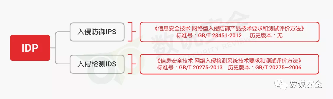
# 1. 入侵检测系统概述**
入侵检测系统(IDS)是一种网络安全工具,用于检测和预防未经授权的访问、滥用、异常或违反安全策略的行为。IDS通过监控网络流量、系统日志和系统活动来识别潜在的威胁,并向管理员发出警报。
IDS可以分为两大类:基于网络的IDS(NIDS)和基于主机的IDS(HIDS)。NIDS监控网络流量,而HIDS监控单个主机的活动。IDS通常使用签名检测、异常检测和行
轨道障碍物智能识别系统开发
轨道障碍物智能识别系统是一种结合了计算机视觉、人工智能和机器学习技术的系统,主要用于监控和管理铁路、航空或航天器的运行安全。它的主要任务是实时检测和分析轨道上的潜在障碍物,如行人、车辆、物体碎片等,以防止这些障碍物对飞行或行驶路径造成威胁。
开发这样的系统主要包括以下几个步骤:
1. **数据收集**:使用高分辨率摄像头、雷达或激光雷达等设备获取轨道周围的实时视频或数据。
2. **图像处理**:对收集到的图像进行预处理,包括去噪、增强和分割,以便更好地提取有用信息。
3. **特征提取**:利用深度学习模型(如卷积神经网络)提取障碍物的特征,如形状、颜色和运动模式。
4. **目标
小波变换在视频压缩中的应用
"多媒体通信技术视频信息压缩与处理(共17张PPT).pptx"
多媒体通信技术涉及的关键领域之一是视频信息压缩与处理,这在现代数字化社会中至关重要,尤其是在传输和存储大量视频数据时。本资料通过17张PPT详细介绍了这一主题,特别是聚焦于小波变换编码和分形编码两种新型的图像压缩技术。
4.5.1 小波变换编码是针对宽带图像数据压缩的一种高效方法。与离散余弦变换(DCT)相比,小波变换能够更好地适应具有复杂结构和高频细节的图像。DCT对于窄带图像信号效果良好,其变换系数主要集中在低频部分,但对于宽带图像,DCT的系数矩阵中的非零系数分布较广,压缩效率相对较低。小波变换则允许在频率上自由伸缩,能够更精确地捕捉图像的局部特征,因此在压缩宽带图像时表现出更高的效率。
小波变换与傅里叶变换有本质的区别。傅里叶变换依赖于一组固定频率的正弦波来表示信号,而小波分析则是通过母小波的不同移位和缩放来表示信号,这种方法对非平稳和局部特征的信号描述更为精确。小波变换的优势在于同时提供了时间和频率域的局部信息,而傅里叶变换只提供频率域信息,却丢失了时间信息的局部化。
在实际应用中,小波变换常常采用八带分解等子带编码方法,将低频部分细化,高频部分则根据需要进行不同程度的分解,以此达到理想的压缩效果。通过改变小波的平移和缩放,可以获取不同分辨率的图像,从而实现按需的图像质量与压缩率的平衡。
4.5.2 分形编码是另一种有效的图像压缩技术,特别适用于处理不规则和自相似的图像特征。分形理论源自自然界的复杂形态,如山脉、云彩和生物组织,它们在不同尺度上表现出相似的结构。通过分形编码,可以将这些复杂的形状和纹理用较少的数据来表示,从而实现高压缩比。分形编码利用了图像中的分形特性,将其转化为分形块,然后进行编码,这在处理具有丰富细节和不规则边缘的图像时尤其有效。
小波变换和分形编码都是多媒体通信技术中视频信息压缩的重要手段,它们分别以不同的方式处理图像数据,旨在减少存储和传输的需求,同时保持图像的质量。这两种技术在现代图像处理、视频编码标准(如JPEG2000)中都有广泛应用。