用verilog写一个数字发射机
时间: 2023-11-07 16:04:42 浏览: 87
好的,我可以帮你回答这个问题。首先需要了解数字发射机的基本原理,数字发射机可以将数字信号转换成模拟信号进行发送,其中需要使用到数字信号处理和调制技术。
在Verilog中,可以使用FPGA或ASIC来实现数字发射机。下面是一个简单的Verilog代码示例,实现数字信号的调制和发送:
```
module digital_transmitter(
input clk, // 时钟信号
input [7:0] data_in, // 输入数字信号
output wire tx_out // 输出模拟信号
);
reg [7:0] counter; // 计数器
reg [7:0] modulated_data; // 调制后的数据
always @(posedge clk) begin
if(counter == 0) begin
modulated_data = data_in; // 对输入数据进行调制
end
counter <= counter + 1; // 计数器自增
end
assign tx_out = modulated_data; // 将调制后的数据输出
endmodule
```
以上代码仅供参考,具体实现需要根据实际需求进行调整和优化。
阅读全文
相关推荐
大家在看
js 在线编辑office source 浏览器在线打开office
onlyffice提供在线编辑office桌面程序和文档服务方式,可以免费在线编辑office,这里提供master分支源码功下载研究
flac3d中文用户手册
flac3d 用户手册,帮助您使用flac3d。
如何降低开关电源纹波噪声
1、什么是纹波?
2、纹波的表示方法
3、纹波的测试
4、纹波噪声的抑制方法
UVM基础学习.ppt
UVM基础学习PPT,讲述了UVM的基础内容,包括UVM框架、agent、sequence、phase等基础内容。
plc 课程设计
里面有plc的运料小车的程序,还有仿真,以及课程设计的格式。
最新推荐
温度传感器(Verilog数字逻辑电路课程设计)
温度传感器的Verilog数字逻辑电路课程设计是一个综合性的项目,涉及到数字系统设计的基本元素,如时序逻辑、接口通信和数据处理。以下是该设计中涉及的主要知识点: 1. **Verilog语言**:Verilog是一种硬件描述语言...
HTML挑战:30天技术学习之旅
资源摘要信息: "desafio-30dias"
标题 "desafio-30dias" 暗示这可能是一个与挑战或训练相关的项目,这在编程和学习新技能的上下文中相当常见。标题中的数字“30”很可能表明这个挑战涉及为期30天的时间框架。此外,由于标题是西班牙语,我们可以推测这个项目可能起源于或至少是针对西班牙语使用者的社区。标题本身没有透露技术上的具体内容,但挑战通常涉及一系列任务,旨在提升个人的某项技能或知识水平。
描述 "desafio-30dias" 并没有提供进一步的信息,它重复了标题的内容。因此,我们不能从中获得关于项目具体细节的额外信息。描述通常用于详细说明项目的性质、目标和期望成果,但由于这里没有具体描述,我们只能依靠标题和相关标签进行推测。
标签 "HTML" 表明这个挑战很可能与HTML(超文本标记语言)有关。HTML是构成网页和网页应用基础的标记语言,用于创建和定义内容的结构、格式和语义。由于标签指定了HTML,我们可以合理假设这个30天挑战的目的是学习或提升HTML技能。它可能包含创建网页、实现网页设计、理解HTML5的新特性等方面的任务。
压缩包子文件的文件名称列表 "desafio-30dias-master" 指向了一个可能包含挑战相关材料的压缩文件。文件名中的“master”表明这可能是一个主文件或包含最终版本材料的文件夹。通常,在版本控制系统如Git中,“master”分支代表项目的主分支,用于存放项目的稳定版本。考虑到这个文件名称的格式,它可能是一个包含所有相关文件和资源的ZIP或RAR压缩文件。
结合这些信息,我们可以推测,这个30天挑战可能涉及了一系列的编程任务和练习,旨在通过实践项目来提高对HTML的理解和应用能力。这些任务可能包括设计和开发静态和动态网页,学习如何使用HTML5增强网页的功能和用户体验,以及如何将HTML与CSS(层叠样式表)和JavaScript等其他技术结合,制作出丰富的交互式网站。
综上所述,这个项目可能是一个为期30天的HTML学习计划,设计给希望提升前端开发能力的开发者,尤其是那些对HTML基础和最新标准感兴趣的人。挑战可能包含了理论学习和实践练习,鼓励参与者通过构建实际项目来学习和巩固知识点。通过这样的学习过程,参与者可以提高在现代网页开发环境中的竞争力,为创建更加复杂和引人入胜的网页打下坚实的基础。
【CodeBlocks精通指南】:一步到位安装wxWidgets库(新手必备)
# 摘要
本文旨在为使用CodeBlocks和wxWidgets库的开发者提供详细的安装、配置、实践操作指南和性能优化建议。文章首先介绍了CodeBlocks和wxWidgets库的基本概念和安装流程,然后深入探讨了CodeBlocks的高级功能定制和wxWidgets的架构特性。随后,通过实践操作章节,指导读者如何创建和运行一个wxWidgets项目,包括界面设计、事件
andorid studio 配置ERROR: Cause: unable to find valid certification path to requested target
### 解决 Android Studio SSL 证书验证问题
当遇到 `unable to find valid certification path` 错误时,这通常意味着 Java 运行环境无法识别服务器提供的 SSL 证书。解决方案涉及更新本地的信任库或调整项目中的网络请求设置。
#### 方法一:安装自定义 CA 证书到 JDK 中
对于企业内部使用的私有 CA 颁发的证书,可以将其导入至 JRE 的信任库中:
1. 获取 `.crt` 或者 `.cer` 文件形式的企业根证书;
2. 使用命令行工具 keytool 将其加入 cacerts 文件内:
```
VC++实现文件顺序读写操作的技巧与实践
资源摘要信息:"vc++文件的顺序读写操作"
在计算机编程中,文件的顺序读写操作是最基础的操作之一,尤其在使用C++语言进行开发时,了解和掌握文件的顺序读写操作是十分重要的。在Microsoft的Visual C++(简称VC++)开发环境中,可以通过标准库中的文件操作函数来实现顺序读写功能。
### 文件顺序读写基础
顺序读写指的是从文件的开始处逐个读取或写入数据,直到文件结束。这与随机读写不同,后者可以任意位置读取或写入数据。顺序读写操作通常用于处理日志文件、文本文件等不需要频繁随机访问的文件。
### VC++中的文件流类
在VC++中,顺序读写操作主要使用的是C++标准库中的fstream类,包括ifstream(用于从文件中读取数据)和ofstream(用于向文件写入数据)两个类。这两个类都是从fstream类继承而来,提供了基本的文件操作功能。
### 实现文件顺序读写操作的步骤
1. **包含必要的头文件**:要进行文件操作,首先需要包含fstream头文件。
```cpp
#include <fstream>
```
2. **创建文件流对象**:创建ifstream或ofstream对象,用于打开文件。
```cpp
ifstream inFile("example.txt"); // 用于读操作
ofstream outFile("example.txt"); // 用于写操作
```
3. **打开文件**:使用文件流对象的成员函数open()来打开文件。如果不需要在创建对象时指定文件路径,也可以在对象创建后调用open()。
```cpp
inFile.open("example.txt", std::ios::in); // 以读模式打开
outFile.open("example.txt", std::ios::out); // 以写模式打开
```
4. **读写数据**:使用文件流对象的成员函数进行数据的读取或写入。对于读操作,可以使用 >> 运算符、get()、read()等方法;对于写操作,可以使用 << 运算符、write()等方法。
```cpp
// 读取操作示例
char c;
while (inFile >> c) {
// 处理读取的数据c
}
// 写入操作示例
const char *text = "Hello, World!";
outFile << text;
```
5. **关闭文件**:操作完成后,应关闭文件,释放资源。
```cpp
inFile.close();
outFile.close();
```
### 文件顺序读写的注意事项
- 在进行文件读写之前,需要确保文件确实存在,且程序有足够的权限对文件进行读写操作。
- 使用文件流进行读写时,应注意文件流的错误状态。例如,在读取完文件后,应检查文件流是否到达文件末尾(failbit)。
- 在写入文件时,如果目标文件不存在,某些open()操作会自动创建文件。如果文件已存在,open()操作则会清空原文件内容,除非使用了追加模式(std::ios::app)。
- 对于大文件的读写,应考虑内存使用情况,避免一次性读取过多数据导致内存溢出。
- 在程序结束前,应该关闭所有打开的文件流。虽然文件流对象的析构函数会自动关闭文件,但显式调用close()是一个好习惯。
### 常用的文件操作函数
- `open()`:打开文件。
- `close()`:关闭文件。
- `read()`:从文件读取数据到缓冲区。
- `write()`:向文件写入数据。
- `tellg()` 和 `tellp()`:分别返回当前读取位置和写入位置。
- `seekg()` 和 `seekp()`:设置文件流的位置。
### 总结
在VC++中实现顺序读写操作,是进行文件处理和数据持久化的基础。通过使用C++的标准库中的fstream类,我们可以方便地进行文件读写操作。掌握文件顺序读写不仅可以帮助我们在实际开发中处理数据文件,还可以加深我们对C++语言和文件I/O操作的理解。需要注意的是,在进行文件操作时,合理管理和异常处理是非常重要的,这有助于确保程序的健壮性和数据的安全。
【大数据时代必备:Hadoop框架深度解析】:掌握核心组件,开启数据科学之旅
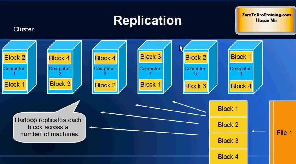
# 摘要
Hadoop作为一个开源的分布式存储和计算框架,在大数据处理领域发挥着举足轻重的作用。本文首先对Hadoop进行了概述,并介绍了其生态系统中的核心组件。深入分
opencv的demo程序
### OpenCV 示例程序
#### 图像读取与显示
下面展示如何使用 Python 接口来加载并显示一张图片:
```python
import cv2
# 加载图像
img = cv2.imread('path_to_image.jpg')
# 创建窗口用于显示图像
cv2.namedWindow('image', cv2.WINDOW_AUTOSIZE)
# 显示图像
cv2.imshow('image', img)
# 等待按键事件
cv2.waitKey(0)
# 销毁所有创建的窗口
cv2.destroyAllWindows()
```
这段代码展示了最基本的图
NeuronTransportIGA: 使用IGA进行神经元材料传输模拟
资源摘要信息:"matlab提取文件要素代码-NeuronTransportIGA:该软件包使用等几何分析(IGA)在神经元的复杂几何形状中执行材料传输模拟"
标题中提到的"NeuronTransportIGA"是一个使用等几何分析(Isogeometric Analysis, IGA)技术的软件包,该技术在处理神经元这样复杂的几何形状时进行材料传输模拟。等几何分析是一种新兴的数值分析方法,它利用与计算机辅助设计(CAD)相同的数学模型,从而提高了在仿真中处理复杂几何结构的精确性和效率。
描述中详细介绍了NeuronTransportIGA软件包的使用流程,其中包括网格生成、控制网格文件的创建和仿真工作的执行。具体步骤包括:
1. 网格生成(Matlab):首先,需要使用Matlab代码对神经元骨架进行平滑处理,并生成用于IGA仿真的六面体控制网格。这里所指的“神经元骨架信息”通常以.swc格式存储,它是一种描述神经元三维形态的文件格式。网格生成依赖于一系列参数,这些参数定义在mesh_parameter.txt文件中。
2. 控制网格文件的创建:根据用户设定的参数,生成的控制网格文件是.vtk格式的,通常用于可视化和分析。其中,controlmesh.vtk就是最终生成的六面体控制网格文件。
在使用过程中,用户需要下载相关代码文件,并放置在meshgeneration目录中。接着,使用TreeSmooth.m代码来平滑输入的神经元骨架信息,并生成一个-smooth.swc文件。TreeSmooth.m脚本允许用户在其中设置平滑参数,影响神经元骨架的平滑程度。
接着,使用Hexmesh_main.m代码来基于平滑后的神经元骨架生成六面体网格。Hexmesh_main.m脚本同样需要用户设置网格参数,以及输入/输出路径,以完成网格的生成和分叉精修。
此外,描述中也提到了需要注意的“笔记”,虽然具体笔记内容未给出,但通常这类笔记会涉及到软件包使用中可能遇到的常见问题、优化提示或特殊设置等。
从标签信息“系统开源”可以得知,NeuronTransportIGA是一个开源软件包。开源意味着用户可以自由使用、修改和分发该软件,这对于学术研究和科学计算是非常有益的,因为它促进了研究者之间的协作和知识共享。
最后,压缩包子文件的文件名称列表为"NeuronTransportIGA-master",这表明了这是一个版本控制的源代码包,可能使用了Git版本控制系统,其中"master"通常是指默认的、稳定的代码分支。
通过上述信息,我们可以了解到NeuronTransportIGA软件包不仅仅是一个工具,它还代表了一个研究领域——即使用数值分析方法对神经元中的物质传输进行模拟。该软件包的开发和维护为神经科学、生物物理学和数值工程等多个学科的研究人员提供了宝贵的资源和便利。
【Linux多系统管理大揭秘】:专家级技巧助你轻松驾驭
# 摘要
本文全面介绍了Linux多系统管理的关键技术和最佳实践。首先概述了多系统管理的基本概念,随后详细探讨了多系统的安装与启动流程,包括系统安装前的准备工作、各主流Linux发行版的安装方法以及启动管理器GRUB2的配置。接下来,文章深入分析了Linux多系统间文件共享与数据迁移的策略,特别是NTFS与Linux文件系统的互操作性和网络文件系统(NFS)的应用。此外,本
fofa和fofa viewer的区别
### Fofa与Fofa Viewer的区别
#### 功能特性对比
FoFA 是一个专注于安全研究的搜索引擎,能够帮助用户发现互联网上的各种资产信息。而 Fofa Viewer 则是一个基于 FoFA 的客户端应用,旨在简化 FoFA 的使用流程并提供更友好的用户体验[^1]。
- **搜索能力**
- FoFA 提供了丰富的语法支持来精确查找特定条件下的网络资源。
- Fofa Viewer 将这些高级功能集成到了图形界面中,使得即使是初学者也能轻松执行复杂的查询操作[^2]。
- **易用性**
- FoFA 主要面向有一定技术背景的安全研究人员和技术爱好者。
-