怎么解决这个问题:Clearance Constraint (Gap=1mil) (inpoly),(All)
时间: 2024-04-14 14:32:13 浏览: 272

设计规则设置-PCB设计流程(AD6.9)
在解决 "Clearance Constraint (Gap=1mil) (inpoly),(All)" 问题时,需要处理的是电路中的间距约束。这个约束要求两个对象之间的间距是1mil。
要解决这个问题,您可以尝试以下步骤:
1. 检查设计规范: 确认设计规范中对于间距约束的要求是否符合。确保了解所使用的设计规范和标准。
2. 调整元件位置: 检查电路中的元件布局,确保它们之间的间距满足指定的要求。可能需要调整元件的位置或重新布局电路。
3. 使用电气设计软件: 使用电气设计软件(如CAD工具)来帮助您分析和调整电路布局。这些工具通常提供自动布线和间距检查的功能,可以帮助您满足约束条件。
4. 手动调整: 如果需要,您可以手动调整元件之间的间距。使用放大镜和精确的测量工具来确保间距达到要求。
5. 与专业人士咨询: 如果您仍然遇到困难,建议咨询专业的电路设计师或工程师,他们可以提供更具体的指导和解决方案。
请注意,具体解决方法可能会因电路设计软件和设计规范的不同而有所变化。所以最好参考所使用软件的文档和手册,以获取更准确的解决方案。
阅读全文
相关推荐
最新推荐
Altium Designer中几种高级的布线规则设置
如果已经存在覆铜,可以通过`Polygon Manager`的`Create Clearance Rule`功能进行后置处理,以确保已敷铜的区域满足设定的间距规则。 通过这些高级布线规则,设计师可以在Altium Designer中实现更精细的控制,从而...
盲孔和埋孔的设计.pdf
总之,盲孔和埋孔技术是现代PCB设计中不可或缺的部分,它们有效地解决了高密度和小型化设计的挑战,同时也对设计师的技能和工具使用提出了更高要求。掌握这些技术,对于提升PCB的性能和可靠性至关重要。
PHP语言基础知识详解及常见功能应用.docx
本文详细介绍了PHP的基本语法、变量类型、运算符号以及文件上传和发邮件功能的实现方法,适合初学者了解和掌握PHP的基础知识。
火炬连体网络在MNIST的2D嵌入实现示例
资源摘要信息:"Siamese网络是一种特殊的神经网络,主要用于度量学习任务中,例如人脸验证、签名识别或任何需要判断两个输入是否相似的场景。本资源中的实现例子是在MNIST数据集上训练的,MNIST是一个包含了手写数字的大型数据集,广泛用于训练各种图像处理系统。在这个例子中,Siamese网络被用来将手写数字图像嵌入到2D空间中,同时保留它们之间的相似性信息。通过这个过程,数字图像能够被映射到一个欧几里得空间,其中相似的图像在空间上彼此接近,不相似的图像则相对远离。
具体到技术层面,Siamese网络由两个相同的子网络构成,这两个子网络共享权重并且并行处理两个不同的输入。在本例中,这两个子网络可能被设计为卷积神经网络(CNN),因为CNN在图像识别任务中表现出色。网络的输入是成对的手写数字图像,输出是一个相似性分数或者距离度量,表明这两个图像是否属于同一类别。
为了训练Siamese网络,需要定义一个损失函数来指导网络学习如何区分相似与不相似的输入对。常见的损失函数包括对比损失(Contrastive Loss)和三元组损失(Triplet Loss)。对比损失函数关注于同一类别的图像对(正样本对)以及不同类别的图像对(负样本对),鼓励网络减小正样本对的距离同时增加负样本对的距离。
在Lua语言环境中,Siamese网络的实现可以通过Lua的深度学习库,如Torch/LuaTorch,来构建。Torch/LuaTorch是一个强大的科学计算框架,它支持GPU加速,广泛应用于机器学习和深度学习领域。通过这个框架,开发者可以使用Lua语言定义模型结构、配置训练过程、执行前向和反向传播算法等。
资源的文件名称列表中的“siamese_network-master”暗示了一个主分支,它可能包含模型定义、训练脚本、测试脚本等。这个主分支中的代码结构可能包括以下部分:
1. 数据加载器(data_loader): 负责加载MNIST数据集并将图像对输入到网络中。
2. 模型定义(model.lua): 定义Siamese网络的结构,包括两个并行的子网络以及最后的相似性度量层。
3. 训练脚本(train.lua): 包含模型训练的过程,如前向传播、损失计算、反向传播和参数更新。
4. 测试脚本(test.lua): 用于评估训练好的模型在验证集或者测试集上的性能。
5. 配置文件(config.lua): 包含了网络结构和训练过程的超参数设置,如学习率、批量大小等。
Siamese网络在实际应用中可以广泛用于各种需要比较两个输入相似性的场合,例如医学图像分析、安全验证系统等。通过本资源中的示例,开发者可以深入理解Siamese网络的工作原理,并在自己的项目中实现类似的网络结构来解决实际问题。"
管理建模和仿真的文件
管理Boualem Benatallah引用此版本:布阿利姆·贝纳塔拉。管理建模和仿真。约瑟夫-傅立叶大学-格勒诺布尔第一大学,1996年。法语。NNT:电话:00345357HAL ID:电话:00345357https://theses.hal.science/tel-003453572008年12月9日提交HAL是一个多学科的开放存取档案馆,用于存放和传播科学研究论文,无论它们是否被公开。论文可以来自法国或国外的教学和研究机构,也可以来自公共或私人研究中心。L’archive ouverte pluridisciplinaire
L2正则化的终极指南:从入门到精通,揭秘机器学习中的性能优化技巧
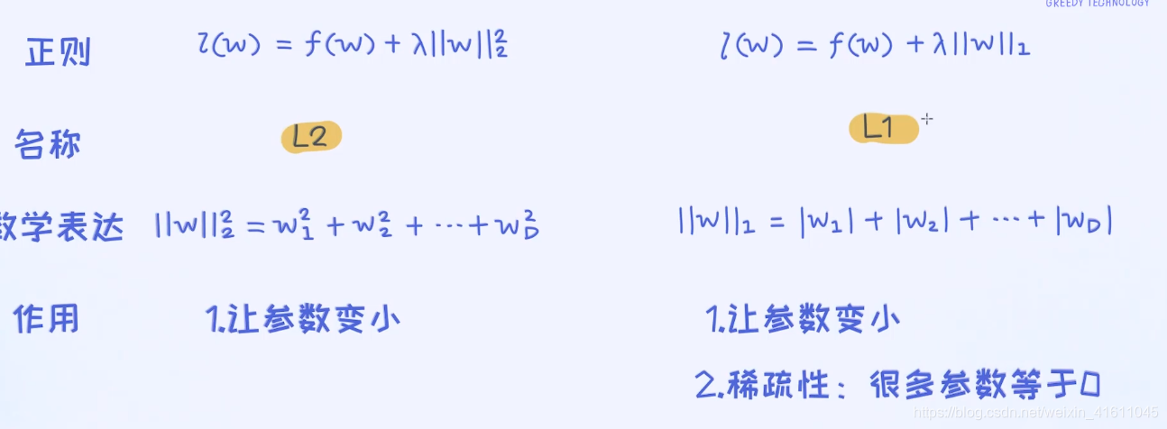
# 1. L2正则化基础概念
在机器学习和统计建模中,L2正则化是一个广泛应用的技巧,用于改进模型的泛化能力。正则化是解决过拟
如何构建一个符合GB/T19716和ISO/IEC13335标准的信息安全事件管理框架,并确保业务连续性规划的有效性?
构建一个符合GB/T19716和ISO/IEC13335标准的信息安全事件管理框架,需要遵循一系列步骤来确保信息系统的安全性和业务连续性规划的有效性。首先,组织需要明确信息安全事件的定义,理解信息安全事态和信息安全事件的区别,并建立事件分类和分级机制。
参考资源链接:[信息安全事件管理:策略与响应指南](https://wenku.csdn.net/doc/5f6b2umknn?spm=1055.2569.3001.10343)
依照GB/T19716标准,组织应制定信息安全事件管理策略,明确组织内各个层级的角色与职责。此外,需要设置信息安全事件响应组(ISIRT),并为其配备必要的资源、
Angular插件增强Application Insights JavaScript SDK功能
资源摘要信息:"Microsoft Application Insights JavaScript SDK-Angular插件"
知识点详细说明:
1. 插件用途与功能:
Microsoft Application Insights JavaScript SDK-Angular插件主要用途在于增强Application Insights的Javascript SDK在Angular应用程序中的功能性。通过使用该插件,开发者可以轻松地在Angular项目中实现对特定事件的监控和数据收集,其中包括:
- 跟踪路由器更改:插件能够检测和报告Angular路由的变化事件,有助于开发者理解用户如何与应用程序的导航功能互动。
- 跟踪未捕获的异常:该插件可以捕获并记录所有在Angular应用中未被捕获的异常,从而帮助开发团队快速定位和解决生产环境中的问题。
2. 兼容性问题:
在使用Angular插件时,必须注意其与es3不兼容的限制。es3(ECMAScript 3)是一种较旧的JavaScript标准,已广泛被es5及更新的标准所替代。因此,当开发Angular应用时,需要确保项目使用的是兼容现代JavaScript标准的构建配置。
3. 安装与入门:
要开始使用Application Insights Angular插件,开发者需要遵循几个简单的步骤:
- 首先,通过npm(Node.js的包管理器)安装Application Insights Angular插件包。具体命令为:npm install @microsoft/applicationinsights-angularplugin-js。
- 接下来,开发者需要在Angular应用的适当组件或服务中设置Application Insights实例。这一过程涉及到了导入相关的类和方法,并根据Application Insights的官方文档进行配置。
4. 基本用法示例:
文档中提到的“基本用法”部分给出的示例代码展示了如何在Angular应用中设置Application Insights实例。示例中首先通过import语句引入了Angular框架的Component装饰器以及Application Insights的类。然后,通过Component装饰器定义了一个Angular组件,这个组件是应用的一个基本单元,负责处理视图和用户交互。在组件类中,开发者可以设置Application Insights的实例,并将插件添加到实例中,从而启用特定的功能。
5. TypeScript标签的含义:
TypeScript是JavaScript的一个超集,它添加了类型系统和一些其他特性,以帮助开发更大型的JavaScript应用。使用TypeScript可以提高代码的可读性和可维护性,并且可以利用TypeScript提供的强类型特性来在编译阶段就发现潜在的错误。文档中提到的标签"TypeScript"强调了该插件及其示例代码是用TypeScript编写的,因此在实际应用中也需要以TypeScript来开发和维护。
6. 压缩包子文件的文件名称列表:
在实际的项目部署中,可能会用到压缩包子文件(通常是一些JavaScript库的压缩和打包后的文件)。在本例中,"applicationinsights-angularplugin-js-main"很可能是该插件主要的入口文件或者压缩包文件的名称。在开发过程中,开发者需要确保引用了正确的文件,以便将插件的功能正确地集成到项目中。
总结而言,Application Insights Angular插件是为了加强在Angular应用中使用Application Insights Javascript SDK的能力,帮助开发者更好地监控和分析应用的运行情况。通过使用该插件,可以跟踪路由器更改和未捕获异常等关键信息。安装与配置过程简单明了,但是需要注意兼容性问题以及正确引用文件,以确保插件能够顺利工作。
"互动学习:行动中的多样性与论文攻读经历"
多样性她- 事实上SCI NCES你的时间表ECOLEDO C Tora SC和NCESPOUR l’Ingén学习互动,互动学习以行动为中心的强化学习学会互动,互动学习,以行动为中心的强化学习计算机科学博士论文于2021年9月28日在Villeneuve d'Asq公开支持马修·瑟林评审团主席法布里斯·勒菲弗尔阿维尼翁大学教授论文指导奥利维尔·皮耶昆谷歌研究教授:智囊团论文联合主任菲利普·普雷教授,大学。里尔/CRISTAL/因里亚报告员奥利维耶·西格德索邦大学报告员卢多维奇·德诺耶教授,Facebook /索邦大学审查员越南圣迈IMT Atlantic高级讲师邀请弗洛里安·斯特鲁布博士,Deepmind对于那些及时看到自己错误的人...3谢谢你首先,我要感谢我的两位博士生导师Olivier和Philippe。奥利维尔,"站在巨人的肩膀上"这句话对你来说完全有意义了。从科学上讲,你知道在这篇论文的(许多)错误中,你是我可以依
L1正则化模型诊断指南:如何检查模型假设与识别异常值(诊断流程+案例研究)

# 1. L1正则化模型概述
L1正则化,也被称为Lasso回归,是一种用于模型特征选择和复杂度控制的方法。它通过在损失函数中加入与模型权重相关的L1惩罚项来实现。L1正则化的作用机制是引导某些模型参数缩小至零,使得模型在学习过程中具有自动特征选择的功能,因此能够产生更加稀疏的模型。本章将从L1正则化的基础概念出发,逐步深入到其在机器学习中的应用和优势