IEEE ANTENNAS AND WIRELESS PROPAGATION LETTERS, VOL. 13, 2014 559
Modeling and Design of Microstrip Patch
Antenna-in-Package for Integrating
the RFIC in the Inner Cavity
Li Li, Xinwei Chen, Yi Zhang, Liping Han, and Wenmei Zhang, Member, IEEE
Abstract—This letter presents the circuit model of the an-
tenna-in-package (AiP) for integrating the RFIC in the inner
cavity. The closed-form expression for the inductance of the
ground via is provided in the case that two ground vias are
arranged under the nonradiating edge of the AiP. The new ex-
pression takes account of the radius and length of the vias, the
relative positions of vias, and the distances between via holes and
the feeding point of the antenna. Based on the circuit model, the
influences of vias on the performance of the AiP are analyzed. It is
found that the bandwidth of the AiP can be effectively improved
by properly arranging two via holes under the nonradiating
edge of the antenna. Finally, an AiP w ith the center frequency of
5.12 GHz is realized, and a bandwidth of 400 MHz is obtained.
The calculated results are in agreement with the simulated and
measured.
Index Terms—Antenna-in-package, equivalent circuit, RF
transceiver, via holes.
I. INTRODUCTION
H
IGHER levels of integration are driven by electrical
performance r equirem ents. Single-chip solutio ns have
the benefit of cost r educt ion and system reliability and there-
fore represent the trend for wireless communications. T he
antenna-in-package (AiP), which is an integrated antenna with
a single-chip RF transceiver on/in a chip package, provides an
advanced system architecture. Zhang proposed the first AiP [1]
and then a series of research about AiP was done [2]–[5]. In
recent years, the studies on AiP mainly focus on the co-design
of antenna and package operating at 60-GHz band due to its
large band w id th an d application in high-speed w ire less com -
munication. CMOS an d LTCC technologies are often used to
fabricate these modules [6]–[9]. Howev er, few papers discuss
the modeling of AiP. In [6], the circuit model of microstrip
patch antenna on the ceram ic land grid array package was
provided.
In this letter, the circuit model of the investigated AiP is
presented. A closed-fo rm expression for the in ductance of the
Manuscript rec eived January 08, 2014; accepted March 10, 2014. Date of
publication March 19, 2014; date of current version April 02, 2014. This work
was supported by the National Science Foundation of China under Grants
61172045 and 61271160, the Natural Science Foundation of Shanxi Province
under Grant 2012011013-3, and the Program for the Top Young Academic
Leaders o f Higher Learning Institutions of Shanxi.
The authors are with College of Physics and Electronics, Shanxi University,
Taiyuan 030006, China (e-mail: zhangwm@sxu.edu.cn).
Color versions of one or more of the figures in this letter are available online
at http://ieeexplore.ieee.org.
Digital Object Identifier 10.1109/LAWP.2014.2312420
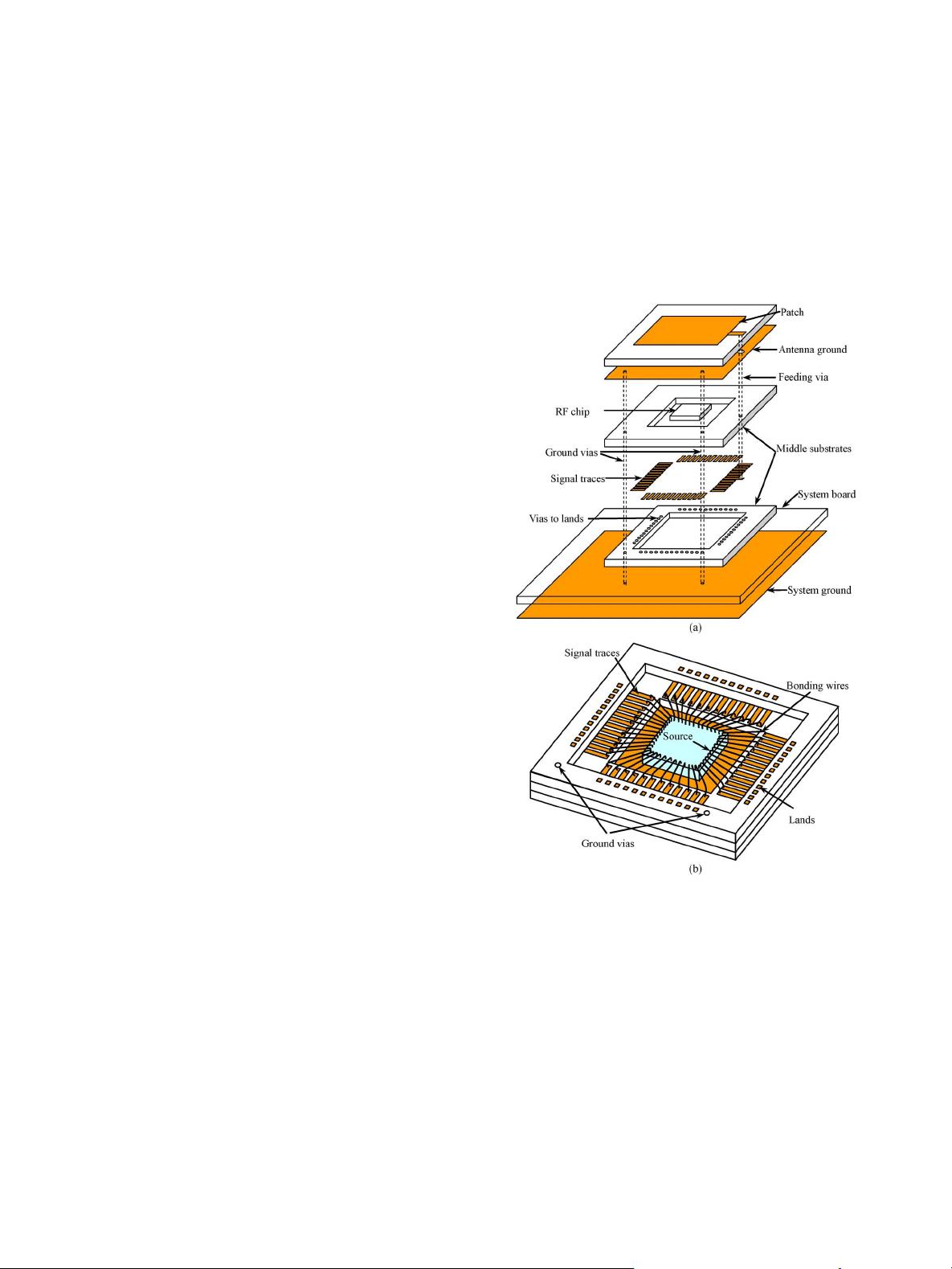
Fig. 1 . Architecture of th e investig ated AiP: (a) explored view; (b) bottom
view.
ground via arranged under the nonradiating edge of the AiP is
deduced. Based on this circuit model, the influences of the posi-
tions of the vias on the AiP are studied. The results indicate the
bandwidth of the investigated AiP can be effectively improved
by arranging two vias prop erly.
II. C
IRCUIT MODEL OF THE AIP
Fig. 1(a) shows the architecture of the investigated AiP. It
consists of three substrate layers and three m etallization layers.
The top m etallization layer is the radiator of the antenna, and
the second and third metallization layers are the antenna ground
and the signal traces, respectively. Under the antenna ground, a
1536-1225 © 2014 IE EE. Personal us e is permitted, but republicatio n / red istribution requires IEEE permission.
See http://www.ieee.org/publications_standards/publications/rights/index.html for more information.


