Monolithic Synthetic Transmission-Line
Leaky-Mode Antenna at THz
C-K C. Tzuang
#1
, Hsien-Shun Wu
#2
, Xinru Li
#3
, and Jianguo Ma
#4
#
School of Electronic Information Engineering, Tianjin University
92 Weijin Road, Nankai District, Tianjin, P.R.China
1
clivetzuang@ieee.org
2
seanwu@ieee.org
3
lixinru@tju.edu.cn
4
majg@tju.edu.cn
Abstract—This paper presents a monolithic leaky EH1-mode
antenna at 400 GHz, incorporating complementary-conducting-
strip synthetic transmission-line structure, aimed to tackle two
CMOS foundry process limiting parameters on conventional
antenna design, first, the thin dielectric substrate height, at the
order of 0.67% operating wavelength, and second, fulfillment of
maximum/minimum metal filling foundry design rule of each
metal layer. A connected array of 11 x 200 cells using the 0.13 μm
1P8M CMOS process, with a unit cell of 16 x 16 μm2, shows good
agreement between measured and simulated input reflection
coefficient, showing return loss of greater than 10 dB between
358 GHz and 400 GHz. Simulated results show peak antenna
gain of 1.589 dB and radiation efficiency of 53.9% in the H-plane,
considering all metal thickness, conductivity, and dielectric losses.
Keywords—CMOS; THz; leaky-mode; transmission line;
I. INTRODUCTION
Recently, the microstrip leaky-wave antenna design
approach attracted renewed interests [1], with their
implementation methods, either in the form of transmission-
line metamaterials [2], or the excitations of microstrip higher-
order modes [3], showing several advantages of the leaky-
mode-based antenna design, largely on the broad frequency-
scanning property and high-gain, high-efficient nature of this
type of antenna [4]-[5].
Most of the printed-circuit-board-based antennas are
limited to the W-band (90-110 GHz) by the photolithographic
resolution in the order of tens of microns [6]. On the other
hand, an increasing demand of integrating a printed antenna
on chip; e.g., an 77 GHz dipole antenna on BiCMOS [7],
manifests a trend to RF front-end system-on-chip, with all RF
signal processing components on the same monolithic
substrate including antennas. However, these monolithic,
integrated antennas often showed poor performance in terms
of gain and efficiency [8], [9]. The micro-machined, cavity-
backed antenna is one example to enhance the antenna
performance by post-processing a silicon foundry technology
[10]. This paper, therefore, aims to tackle the issue of poorer
antenna efficiency resulting from the relatively thin substrate
height as observed in most silicon foundry processes, typically
in the order of less than 0.5% operating wavelength [11].
Furthermore, every CMOS foundry mandates the satisfaction
of metal density filling rule, to ensure the surface flatness,
required for high-precision sub-micron photolithography
technology. This paper proposes the use of synthetic
transmission-line (TL) called, complementary-conducting-
strip transmission line (CCS TL), using a unit cell typically in
the order of one thousandth operating wavelength [12], from
which a monolithic leaky EH1-mode antenna is built, tested,
and verified. Section II reports the designs of the unit cell and
the leaky-mode antenna, respectively. Section III investigates
the dispersive modal characteristics of the synthetic
transmission-line shown in Section II, followed by
experimental validation of simulated input return loss using
full-wave analyses (HFSS
TM
) considering all material
constants and structural parameters. Section V, therefore
reports and discusses the simulated radiation patterns,
scanning frequency property, pertinent to the nature of leaky-
mode radiation characteristics, followed by the report of
unique features of the proposed design. Section VI concludes
the paper.
II.
ANTENNA DESIGN
A. Unit Cell and Transmission Line
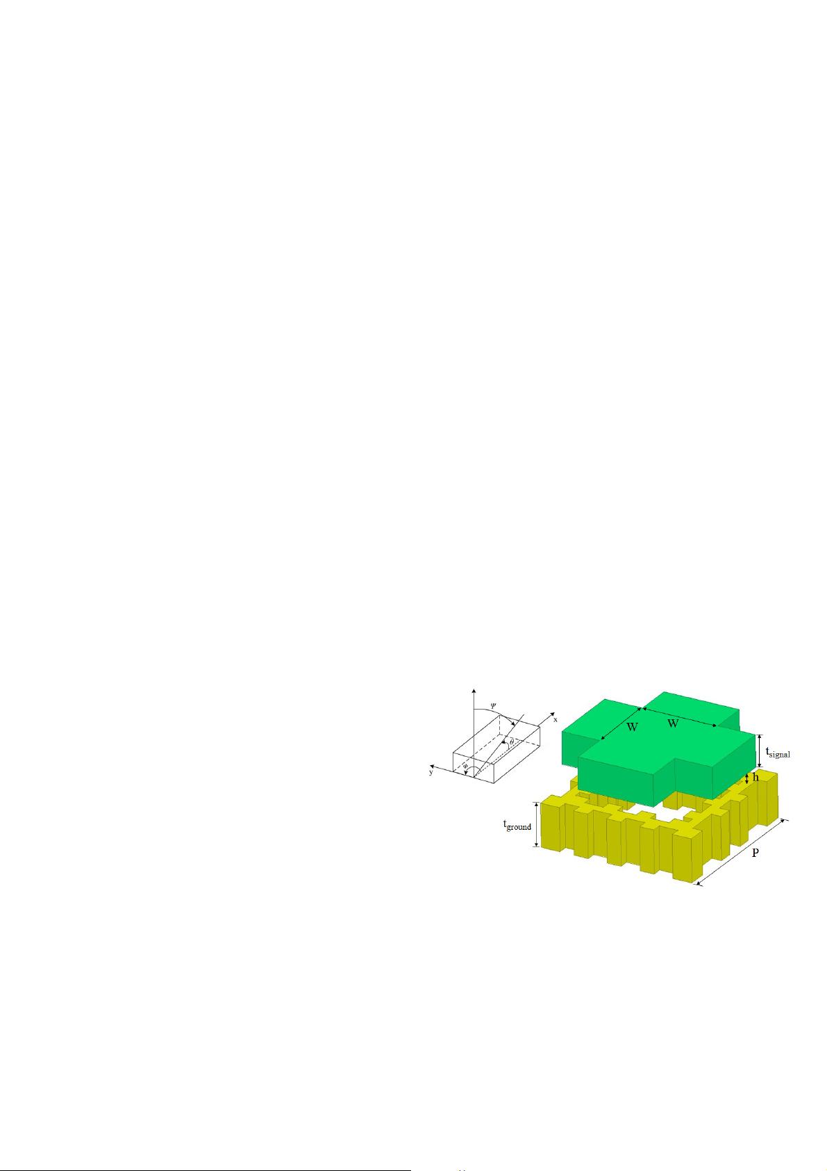
Fig. 1 The unit cell structure of periodicity P, bottom meshed ground plane of
simplified view replacing via-connected layers by solid metals, and the top
complementary-metal-strip of four connecting arms. P = 16 μm, W=8 μm, h =
5.7 μm, t
ground
= 2.0 μm, t
signal
= 3.3 μm. Conductivity of the signal trace =
5.8275×10
7
S/m, conductivity of the ground plane = 4.6168×10
7
S/m, ε
r
of
dielectric layer = 4.0, conductivity of the silicon substrate = 11.0 S/m.
978-2-87487-031-6 © 2013 EuMA 7
-
10 Oct 2013, Nuremberg, Germany
Proceedings of the 43rd European Microwave Conference
499


