"TPS54560-Q1-车规级.pdf: 高效能转换器效率测试结果"
版权申诉
114 浏览量
更新于2024-03-02
收藏 2.18MB PDF 举报
The TPS54560-Q1 is a automotive-grade step-down voltage regulator designed for use in vehicle applications. This regulator offers high efficiency and a wide input voltage range, making it ideal for a variety of automotive systems. The efficiency of the TPS54560-Q1 improves as the output current increases, with performance optimized for input voltages of 12V, 36V, and 60V.
With its robust design and automotive-grade certification, the TPS54560-Q1 is a reliable and durable solution for power management in automotive systems. Its compact size and high efficiency make it well-suited for use in space-constrained applications where energy efficiency is a priority.
The TPS54560-Q1 features a wide input voltage range, allowing it to adapt to changing conditions in automotive systems. It also includes protection features such as overcurrent and overtemperature protection, ensuring the safe and reliable operation of the regulator in harsh automotive environments.
In conclusion, the TPS54560-Q1 is a high-performance and reliable automotive-grade voltage regulator that offers high efficiency and a wide input voltage range. Its compact size and robust design make it an ideal choice for power management in automotive systems, providing a dependable and efficient solution for vehicle applications.
0
1
2
3
4
5
6
7
8
9
10
100
300
500
700
900
1100
1300
1500
1700
1900
2100
2300
2500
Soft-Start Time (ms)
Switching Frequency (kHz)
C045
4.6
4.7
4.8
4.9
5
5.1
5.2
5.3
5.4
5.5
5.6
0 0.05 0.1 0.15 0.2 0.25 0.3 0.35 0.4 0.45 0.5
V
IN
(V)
Output Current (A)
Start
Stop
C046
Dropout
Voltage
Dropout
Voltage
3.7
3.8
3.9
4.0
4.1
4.2
4.3
4.4
4.5
±50 ±25 0 25 50 75 100 125 150
V
IN
(V)
T
J
- Junction Temperature (ƒC)
UVLO Start Switching
UVLO Stop Switching
C044
1.8
1.9
2.0
2.1
2.2
2.3
2.4
2.5
2.6
±50 ±25 0 25 50 75 100 125 150
V
I
- BOOT-PH (V)
T
J
- Junction Temperature (ƒC)
BOOT-PH UVLO Falling
BOOT-PH UVLO Rising
C043
9
TPS54560-Q1
www.ti.com.cn
ZHCSBN7A –SEPTEMBER 2013–REVISED DECEMBER 2014
Copyright © 2013–2014, Texas Instruments Incorporated
Typical Characteristics (continued)
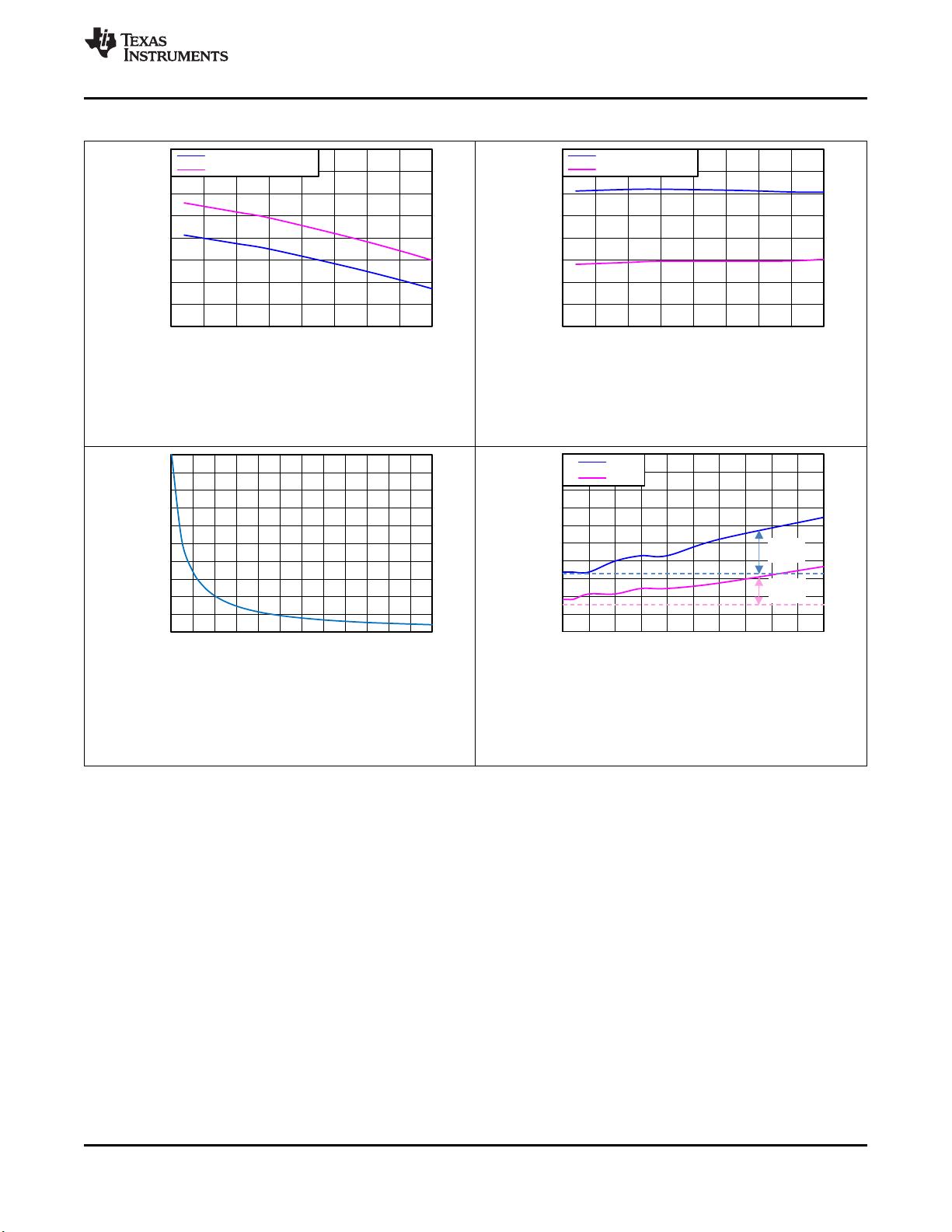
Figure 19. BOOT-SW UVLO vs Junction Temperature
Figure 20. Input Voltage UVLO vs Junction Temperature
Figure 21. Soft-Start Time vs Switching Frequency
Figure 22. 5 V Start and Stop Voltage (see Low Dropout
Operation and Bootstrap Voltage (BOOT))

剩余46页未读,继续阅读
2023-07-22 上传
2023-07-22 上传
2022-10-24 上传
2022-11-17 上传
2022-11-16 上传
2022-12-16 上传
2022-11-16 上传
2022-11-20 上传
2022-11-16 上传

RedCar
- 粉丝: 57
- 资源: 2108
 我的内容管理
展开
我的内容管理
展开


