2023 IEEE 固态电路国际会议专题论文集
需积分: 5 98 浏览量
更新于2024-06-15
收藏 123.25MB PDF 举报
"JSSC 2023.11 all papers"
这是一期关于《IEEE固态电路杂志》(Journal of Solid-State Circuits,简称JSSC)的特刊,发布于2023年11月。JSSC是固态电路领域的权威期刊,涵盖了广泛的电子电路设计和技术,包括模拟、数字、混合信号和存储器集成电路。这期特刊重点关注2023年IEEE国际固态电路会议(ISSCC),这是一个展示固态电路最新进展的全球性重要会议。
本期特刊由D. Sylvester成为新的副编辑,并由M. Kiani和K. Sengupta撰写客座编辑序言,介绍2023年ISSCC的特色和重要性。该特刊包含了多篇技术论文,展示了固态电路在各个方面的创新。
首先,有一篇论文介绍了采用三片晶圆堆叠的混合型15兆像素CIS(互补金属氧化物半导体图像传感器)+1兆像素EVS(事件视觉传感器)的设计,具备4.6-G事件/秒的读出速度、像素内时钟数字转换器以及片上图像信号处理器和环境光传感器功能。这个设计展示了高集成度和高速数据处理能力在图像传感器领域的应用。
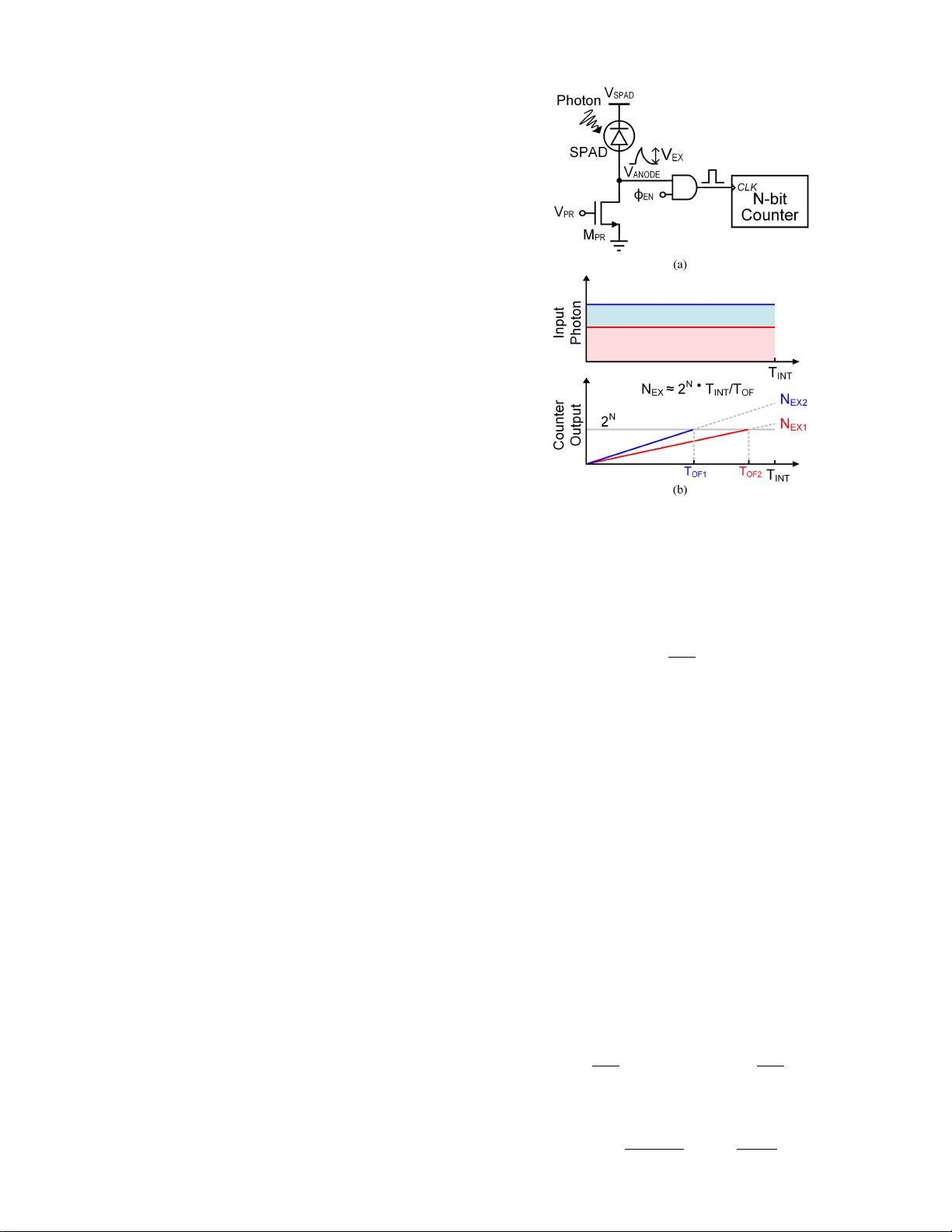
其次,还有一篇论文描述了一个具有113.3-dB动态范围、600帧/秒的SPAD(单光子雪崩二极管)X射线探测器,其特点是无缝全局快门和时间编码扩展计数器。这一创新技术对于高精度成像和医疗检测具有重大意义。
此外,还有一款低刺激散射像素共享的次视网膜假体系统级芯片(SoC)被提出,它采用了基于时间的光电二极管感应和像素级动态电压缩放。这种设计旨在提高人工视网膜假体的性能,为视力受损者提供更好的视觉恢复可能性。
这些论文展示了固态电路在成像、医疗应用、以及生物医学工程等领域的前沿进展,涵盖了从新器件架构到高级信号处理算法的各种创新。通过JSSC 2023.11特刊,读者可以了解到固态电路技术的最新趋势和发展,这对于相关领域的研究者、工程师和学生来说是极其宝贵的资源。
2962 IEEE JOURNAL OF SOLID-STATE CIRCUITS, VOL. 58, NO. 11, NOVEMBER 2023
V. CONCLUSION
We have introduced a state-of-the-art hybrid EVS/CIS
image sensor. This was achieved using advanced three-
wafer-stacking technology. The hybrid sensor simplifies
synchronization between EVS and CIS compared with a
two-sensor solution. Furthermore, a hybrid sensor avoids
parallax/occlusion errors and requires only one package and
lens. This enables new use-cases such as rolling-shutter
correction or deblur image enhancement, video frame inter-
polation for slow motion, and simultaneous localization and
mapping.
The CIS pixel array sacrifices only one out of 16 color
channels for EVS functionality which achieves comparable
image quality to the state-of-the-art sparse phase-detection
autofocus systems. The EVS pixel was evaluated at a linear
NCT setting of 15% achieving a CTNU of ∼3% being
comparable to stand-alone EVS sensors. Very low noise of
<1 Hz is reported.
Conversely to arbiter-based readout, the content-aware scan
operation achieves fair, low-latency readout through the bypass
of rows and columns without events and a skip function that
only reads out the first and last events of a connected group of
events having the same polarity. Using these methodologies,
we report a maximum event rate of up to 4.6 GEps. The power
consumption at 55 pJ/Event outperforms recently published
stand-alone EVS sensors with at least VGA resolution by
up to 200% depending on the actual event distribution in
the array. We thus report three leading figures of merits.
The first describes the multiplication of event pixel resolu-
tion times event rate yielding 4.4 MP × GEps. The second
normalizes the first FOM by the required power achieving
0.08 MP × GEps/pJ. And the last FOM multiplies CIS and
EVS resolution as well as the CIS frame rate and EVS event
rate to form a hybrid measure of 1200 MP
2
×frames/s × GEps.
REFERENCES
[1] P. Lichtensteiner, “An AER temporal contrast vision sensor,”
Ph.D. thesis, ETH, Zürich, Switzerland, 2006.
[2] G. Gallego et al., “Event-based vision: A survey,” IEEE Trans. Pat-
tern Anal. Mach. Intell., vol. 44, no. 1, pp. 154–180, Jan. 2022, doi:
10.1109/TPAMI.2020.3008413.
[3] T. Haruta et al., “A 1/2.3inch 20Mpixel 3-layer stacked CMOS image
sensor with DRAM,” in IEEE Int. Solid-State Circuits Conf. (ISSCC)
Dig. Tech. Papers, San Francisco, CA, USA, Feb. 2017, pp. 76–77, doi:
10.1109/ISSCC.2017.7870268.
[4] C. Posch, D. Matolin, and R. Wohlgenannt, “An asynchronous
time-based image sensor,” in Proc. IEEE Int. Symp. Circuits
Syst., Seattle, WA, USA, May 2008, pp. 2130–2133, doi:
10.1109/ISCAS.2008.4541871.
[5] C. Brandli, R. Berner, M. Yang, S.-C. Liu, and T. Delbruck, “A 240×180
130 dB 3 µs latency global shutter spatiotemporal vision sensor,” IEEE
J. Solid-State Circuits, vol. 49, no. 10, pp. 2333–2341, Oct. 2014, doi:
10.1109/JSSC.2014.2342715.
[6] C. Li et al., “Design of an RGBW color VGA rolling and global
shutter dynamic and active-pixel vision sensor,” in Proc. IEEE Int. Symp.
Circuits Syst. (ISCAS), Lisbon, Portugal, May 2015, pp. 718–721, doi:
10.1109/ISCAS.2015.7168734.
[7] T. Finateu et al., “A 1280 × 720 back-illuminated stacked temporal
contrast event-based vision sensor with 4.86 µm pixels, 1.066GEPS
readout, programmable event-rate controller and compressive data-
formatting pipeline,” in IEEE Int. Solid-State Circuits Conf. (ISSCC)
Dig. Tech. Papers, San Francisco, CA, USA, Feb. 2020, pp. 112–114,
doi: 10.1109/ISSCC19947.2020.9063149.
[8] B. Son et al., “A 640 × 480 dynamic vision sensor with a 9 µm pixel
and 300Meps address-event representation,” in IEEE Int. Solid-State
Circuits Conf. (ISSCC) Dig. Tech. Papers, Feb. 2017, pp. 66–67, doi:
10.1109/ISSCC.2017.7870263.
[9] Y. Suh et al., “A 1280 × 960 dynamic vision sensor with a 4.95-µm
pixel pitch and motion artifact minimization,” in Proc. IEEE Int.
Symp. Circuits Syst. (ISCAS), Seville, Spain, Oct. 2020, pp. 1–5, doi:
10.1109/ISCAS45731.2020.9180436.
[10] S. Chen, “Development of event-based sensor and applications,” in
Proc. Conf. Comput. Vis. Pattern Recognit. (CVPR), 2021, pp. 1–17.
Accessed: Aug. 22, 2022. [Online]. Available: https://tub-rip.github.io/
eventvision2021/slides/CVPRW21_Shoushun_Chen.pdf
[11] iniVation. Specifications—Current Models. Accessed: Aug. 22, 2022.
[Online]. Available: https://inivation.com/wp-content/uploads/2021/
08/2021-08-iniVation-devices-Specifications.pdf
[12] C. Li, L. Longinotti, F. Corradi, and T. Delbruck, “A 132 by 104 10 µm-
pixel 250 µW 1kefps dynamic vision sensor with pixel-parallel noise
and 107 spatial redundancy suppression,” in Proc. Int. Image Sensor
Workshop (IISW), Snowbird, UT, USA, 2019, p. 16.
[13] M. Guo et al., “A 3-wafer-stacked hybrid 15MPixel CIS +
1 MPixel EVS with 4.6G event/s readout, in-pixel TDC and on-
chip ISP and ESP function,” in IEEE Int. Solid-State Circuits
Conf. (ISSCC) Dig. Tech. Papers, Feb. 2023, pp. 90–92, doi:
10.1109/ISSCC42615.2023.10067476.
[14] Y. Yaffe et al., “Dynamic vision sensor—The road to market,” in Proc.
Int. Conf. Robot. Automat. (ICRA), 2017. Accessed: May 3, 2023.
[Online]. Available: https://rpg.ifi.uzh.ch/docs/ICRA17workshop/
Samsung.pdf
[15] K. Kodama et al., “1.22 µm 35.6Mpixel RGB hybrid event-based vision
sensor with 4.88 µm-pitch event pixels and up to 10K event frame
rate by adaptive control on event sparsity,” in IEEE Int. Solid-State
Circuits Conf. (ISSCC) Dig. Tech. Papers, Feb. 2023, pp. 92–93, doi:
10.1109/ISSCC42615.2023.10067520.
[16] A. Niwa et al., “A 2.97 µm-pitch event-based vision sensor with shared
pixel front-end circuitry and low-noise intensity readout mode,” in IEEE
Int. Solid-State Circuits Conf. (ISSCC) Dig. Tech. Papers, Feb. 2023,
pp. 94–95, doi: 10.1109/ISSCC42615.2023.10067566.
[17] A. Suess et al., “Physical modeling and parameter extraction for event-
based vision sensors,” in Proc. IISS Int. Image Sensor Workshop (IISW),
Edinburgh, U.K., 2023, p. R5.5.
Menghan Guo received the M.E. degree in circuits
and systems from Southeast University, Nanjing,
China, in 2013.
From 2013 to 2017, he was a Research
Associate with Nanyang Technological University,
Singapore. In 2017, he joined CelePixel Technolo-
gies, Shanghai, China, as the IC Design Manager
for smart vision sensors in 2017, and he is currently
with OMNIVISION, Shanghai. His research inter-
ests mainly focus on the design of event-based vision
sensor.
Shoushun Chen (Senior Member, IEEE) received
the B.S. degree from Peking University, Beijing,
China, in 2000, the M.E. degree from the Chinese
Academy of Sciences, Beijing, in 2003, and the
Ph.D. degree from the Hong Kong University of
Science and Technology, Hong Kong, in 2007.
He held postdoctoral positions with the Hong
Kong University of Science and Technology and
Yale University, New Haven, CT, USA. From July
2009 to April 2023, he was an Assistant Professor
and later promoted to tenured Associate Professor
with Nanyang Technological University, Singapore. He is the Founder of
CelePixel Technology, Shanghai, China, which was acquired by OMNIVI-
SION, Shanghai, in 2020. His research focuses on various areas, including
smart vision sensors, motion detection sensors, energy-efficient algorithms for
bioinspired vision and analog/mixed-signal VLSI circuits and systems.
Dr. Chen serves as the Chair of the Technical Committee of Sensory Systems
for the IEEE Circuits and Systems Society (CASS).

剩余343页未读,继续阅读
2024-01-28 上传
2024-01-28 上传
2024-01-28 上传
2024-03-18 上传
2024-03-18 上传
2024-03-18 上传
2024-03-18 上传
2024-01-28 上传

netshell
- 粉丝: 11
- 资源: 185
 我的内容管理
展开
我的内容管理
展开


最新资源
- MATLAB新功能:Multi-frame ViewRGB制作彩色图阴影
- XKCD Substitutions 3-crx插件:创新的网页文字替换工具
- Python实现8位等离子效果开源项目plasma.py解读
- 维护商店移动应用:基于PhoneGap的移动API应用
- Laravel-Admin的Redis Manager扩展使用教程
- Jekyll代理主题使用指南及文件结构解析
- cPanel中PHP多版本插件的安装与配置指南
- 深入探讨React和Typescript在Alias kopio游戏中的应用
- node.js OSC服务器实现:Gibber消息转换技术解析
- 体验最新升级版的mdbootstrap pro 6.1.0组件库
- 超市盘点过机系统实现与delphi应用
- Boogle: 探索 Python 编程的 Boggle 仿制品
- C++实现的Physics2D简易2D物理模拟
- 傅里叶级数在分数阶微分积分计算中的应用与实现
- Windows Phone与PhoneGap应用隔离存储文件访问方法
- iso8601-interval-recurrence:掌握ISO8601日期范围与重复间隔检查
