数字设计基础与实践:探索硬件世界
"Digital Design Principles and Practices,3rd (数字设计原理与实践(第三版)英文版)"
本书《数字设计原理与实践》是John F. Wakerly所著的第三版,由Prentice Hall在1999年出版,以PDF格式提供,无加密。该书主要针对的是计算机科学和电子工程领域的学生,无论是对计算机硬件有疑问的软件专业学生,还是对模拟电子和电路设计有一定了解的电气工程学生,都可以从中受益。
1.1 关于数字系统
本书的开篇介绍了数字系统的基本概念。数字设计是理解和创建数字电路及子系统的基石,这些电路和子系统构成了我们现代电子设备的核心。作者旨在从一个相对基础的水平出发,帮助读者理解如何设计这些复杂的系统。
1.2 数字逻辑
书中会深入讲解数字逻辑的基础,包括布尔代数、基本逻辑门(如AND、OR、NOT)、组合逻辑电路以及时序逻辑电路的设计。这些基础知识是数字设计的根基,能够帮助读者理解如何用简单的逻辑元素构建复杂的逻辑功能。
1.3 数字数据表示
数字数据在计算机中是如何表示的也是本书的重要内容。这包括二进制、八进制、十六进制等不同进制转换,以及位、字节、字的构成,还有数值、字符、浮点数的存储方式。
1.4 芯片和集成电路
书中会介绍不同类型的半导体材料和器件,如二极管、晶体管,以及它们在数字电路中的应用。此外,大规模集成电路(VLSI)和微处理器的工作原理也会被讨论,这将使读者理解现代计算机硬件的内部运作。
1.5 数字电路设计方法
在理论基础上,作者会分享实际的数字电路设计方法,包括硬件描述语言(HDL,如Verilog和VHDL)的使用,以及如何通过逻辑综合和布局布线工具将设计转化为实际电路。
1.6 实验与项目
为了巩固理论知识,书中通常包含实验指导和项目建议,鼓励读者动手实践,通过实际操作来加深对理论的理解。
1.7 当前技术趋势
考虑到技术的快速发展,书中会讨论当前的数字设计趋势,如可编程逻辑器件(FPGA)、嵌入式系统、高速通信接口和低功耗设计等,让读者了解数字设计领域的最新发展。
通过本书的学习,读者不仅可以掌握数字设计的基本原理,还能了解实际设计过程中的挑战和解决方案,以及如何与不断变化的技术环境保持同步。作者采用的亲和性叙述方式,旨在让读者感觉如同共同探索学习过程,从而更有效地掌握这一领域知识。
16 Chapter 1 Introduction
DO NOT COPY
DO NOT COPY
DO NOT COPY
DO NOT COPY
DO NOT COPY
DO NOT COPY
DO NOT COPY
DO NOT COPY
DO NOT COPY
Copyright © 1999 by John F. Wakerly Copying Prohibited
Proponents of one approach or the other used to get into “religious” argu-
ments over which way was better, but the largest manufacturer of large
programmable logic devices, Xilinx Corporation, acknowledges that there is a
place for both approaches and manufactures both types of devices. What’s more
important than chip architecture is that both approaches support a style of design
in which products can be moved from design concept to prototype and produc-
tion in a very period of time short time.
Also important in achieving short “time-to-market” for all kinds of PLD-
based products is the use of HDLs in their design. Languages like ABEL and
VHDL, and their accompanying software tools, allow a design to be compiled,
synthesized, and downloaded into a PLD, CPLD, or FPGA literally in minutes.
The power of highly structured, hierarchical languages like VHDL is especially
important in helping designers utilize the hundreds of thousands or millions of
gates that are provided in the largest CPLDs and FPGAs.
1.8 Application-Specific ICs
Perhaps the most interesting developments in IC technology for the average
digital designer are not the ever-increasing chip sizes, but the ever-increasing
opportunities to “design your own chip.” Chips designed for a particular, limited
product or application are called
semicustom ICs
or
application-specific ICs
(ASICs)
. ASICs generally reduce the total component and manufacturing cost of
a product by reducing chip count, physical size, and power consumption, and
they often provide higher performance.
The
nonrecurring engineering (NRE) cost
for designing an ASIC can
exceed the cost of a discrete design by $5,000 to $250,000 or more. NRE charges
are paid to the IC manufacturer and others who are responsible for designing the
PLD PLD PLD PLD
PLD PLD PLD PLD
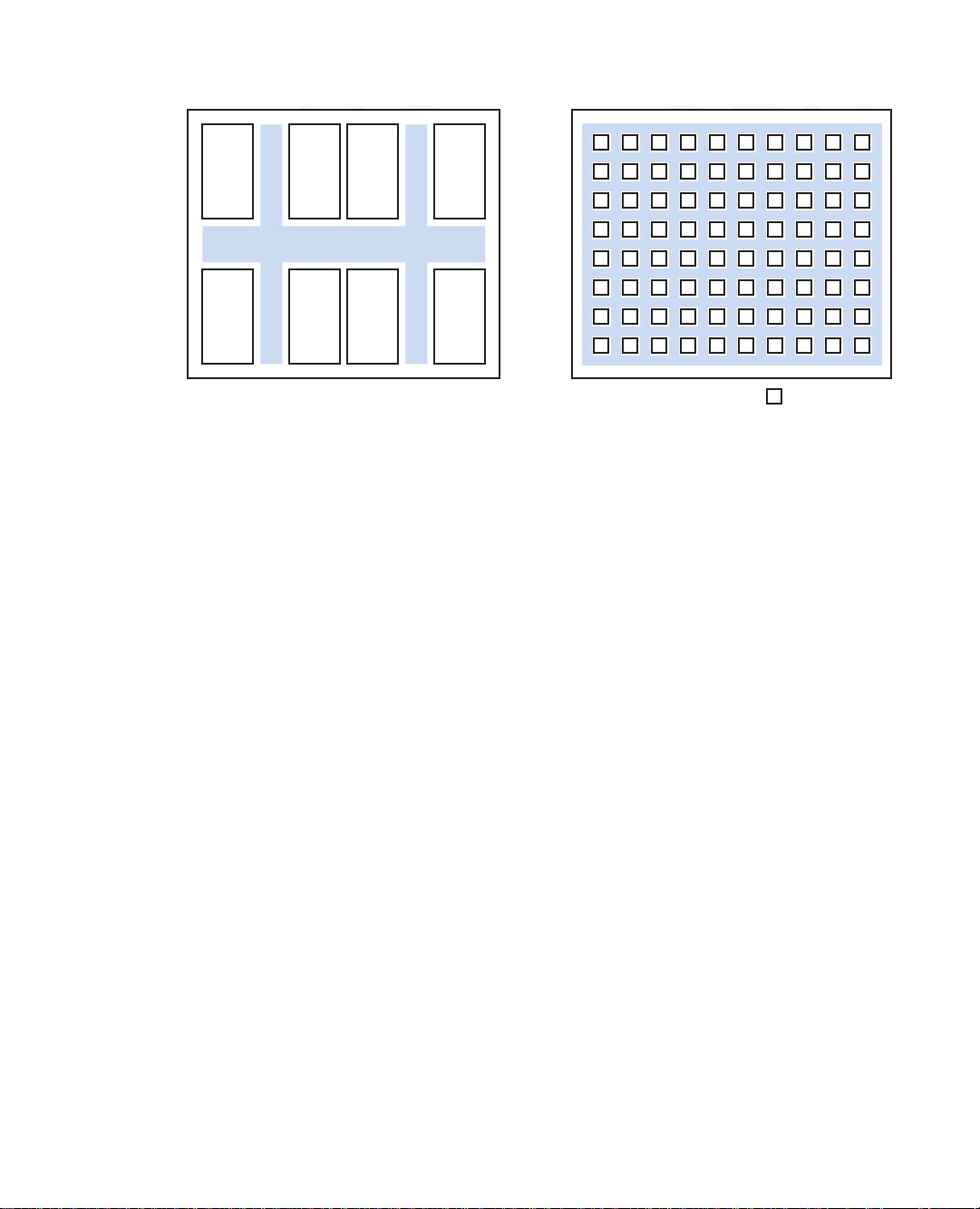
Programmable Interconnect
(a) (b) = logic block
Figure 1-6
Large programmable-logic-device scaling approaches: (a) CPLD; (b) FPGA.
semicustom IC
application-specific IC
(ASIC)
nonrecurring
engineering (NRE)
cost


剩余793页未读,继续阅读
相关推荐


405 浏览量


kevin_liuk
- 粉丝: 0
 我的内容管理
展开
我的内容管理
展开


最新资源
- VB通过Modbus协议控制三菱PLC通讯实操指南
- simfinapi:R语言中简化SimFin数据获取与分析的包
- LabVIEW温度控制上位机程序开发指南
- 西门子工业网络通信实例解析与CP243-1应用
- 清华紫光全能王V9.1软件深度体验与功能解析
- VB实现Access数据库数据同步操作指南
- VB实现MSChart绘制实时监控曲线
- VC6.0通过实例深入访问Excel文件技巧
- 自动机可视化工具:编程语言与正则表达式的图形化解释
- 赛义德·莫比尼:揭秘其开创性技术成果
- 微信小程序开发教程:如何实现模仿ofo共享单车应用
- TrueTable在Windows10 64位及CAD2007中的完美适配
- 图解Win7搭建IIS7+PHP+MySQL+phpMyAdmin教程
- C#与LabVIEW联合采集NI设备的电压电流信号并创建Excel文件
- LP1800-3最小系统官方资料压缩包
- Linksys WUSB54GG无线网卡驱动程序下载指南
