BCM2835 ARM单板电脑处理器外围设备与接口详解
本文档是关于BCM2835 ARM外设的详细指南,由英国的Broadcom Corporation提供。BCM2835是一款针对单板计算机设计的处理器,主要应用于教育、嵌入式系统和原型开发等领域。文档主要涵盖了四个核心部分:介绍、辅助接口(UART1 & SPI1, SPI2)、BSC(Base System Controller)以及DMA控制器。
1. **介绍**:
- 提供了BCM2835的整体概述,强调其在Linux内核中的标准地址映射。
- 内容包括地址映射的图解概述,区分了ARM虚拟地址(适用于标准Linux内核)和物理地址,以及总线地址。
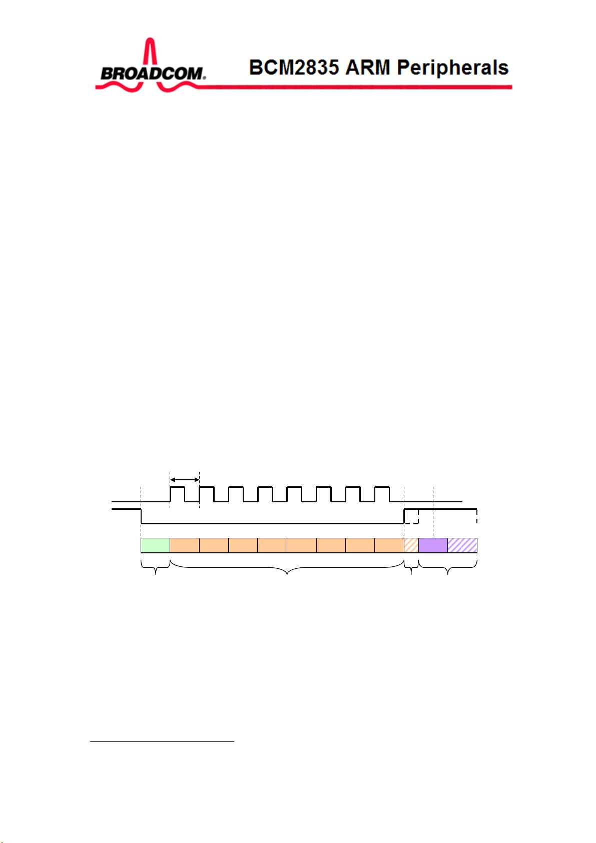
2. **辅助接口**:
- UART1 & SPI1 和 SPI2 是文档的重点,涉及它们的功能、注册寄存器以及操作细节。
- MiniUART(一种简化版的UART)详细解释了其内部实现和寄存器结构,支持中断处理和长数据流传输。
- Universal SPI Master(双通道)则介绍了SPI接口的具体实现,包括中断机制、处理长位流以及相应的寄存器配置。
3. **BSC (Base System Controller)**:
- BSC是BCM2835的核心组件之一,负责管理CPU与外设之间的通信。
- 文档提供了BSC的介绍和寄存器视图,10位地址寻址模式也是其中的一部分。
4. **DMA Controller**:
- DMA控制器用于数据的高速传输,不占用CPU处理时间。
- 介绍部分概述了DMA的功能,随后详细列出了DMA通道寄存器的地址映射。
- 还讨论了AXI Burst技术,提高数据传输效率,并包含错误处理机制。
这篇文档为开发者提供了BCM2835处理器上关键外设的深入理解,包括地址映射、通信接口规范和硬件控制逻辑,有助于进行高效且兼容Linux的系统设计和开发工作。对于使用BCM2835的工程师来说,这是不可或缺的技术参考材料。
06 February 2012 Broadcom Europe Ltd. 406 Science Park Milton Road Cambridge CB4 0WW Page 16
© 2012 Broadcom Corporation. All rights reserved
AUX_MU_SCRATCH Register (0x7E21 505C)
S
YNOPSIS
The
AUX_MU_SCRATCH
is a single byte storage.
Bit(s) Field Name Description Type
Reset
31:8
Reserved, write zero, read as don’t care
7:0 Scratch
One whole byte extra on top of the 134217728
provided by the SDC
R/W 0
AUX_MU_CNTL_REG Register (0x7E21 5060)
S
YNOPSIS
The
AUX_MU_CNTL_REG
provides access to some extra useful and nice features not
found on a normal 16550 UART .
Bit(s) Field Name Description Type
Reset
31:8
Reserved, write zero, read as don’t care
7
CTS assert
level
This bit allows one to invert the CTS auto flow
operation polarity.
If set the CTS auto flow assert level is low*
If clear the CTS auto flow assert level is high*
R/W 0
6
RTS assert
level
This bit allows one to invert the RTS auto flow
operation polarity.
If set the RTS auto flow assert level is low*
If clear the RTS auto flow assert level is high*
R/W 0
5:4
RTS AUTO
flow level
These two bits specify at what receiver FIFO level the
RTS line is de-asserted in auto-flow mode.
00 : De-assert RTS when the receive FIFO has 3
empty spaces left.
01 : De-assert RTS when the receive FIFO has 2
empty spaces left.
10 : De-assert RTS when the receive FIFO has 1
empty space left.
11 : De-assert RTS when the receive FIFO has 4
empty spaces left.
R/W 0
3
Enable
transmit Auto
flow-control
using CTS
If this bit is set the transmitter will stop if the CTS
line is de-asserted.
If this bit is clear the transmitter will ignore the status
of the CTS line
R/W 0
剩余204页未读,继续阅读
2016-01-06 上传
2023-07-28 上传
2023-06-03 上传
2023-06-08 上传
2024-11-05 上传
2023-05-24 上传
2023-04-07 上传

zys_ffmpeg
- 粉丝: 0
- 资源: 2
 我的内容管理
展开
我的内容管理
展开


最新资源
- Elasticsearch核心改进:实现Translog与索引线程分离
- 分享个人Vim与Git配置文件管理经验
- 文本动画新体验:textillate插件功能介绍
- Python图像处理库Pillow 2.5.2版本发布
- DeepClassifier:简化文本分类任务的深度学习库
- Java领域恩舒技术深度解析
- 渲染jquery-mentions的markdown-it-jquery-mention插件
- CompbuildREDUX:探索Minecraft的现实主义纹理包
- Nest框架的入门教程与部署指南
- Slack黑暗主题脚本教程:简易安装指南
- JavaScript开发进阶:探索develop-it-master项目
- SafeStbImageSharp:提升安全性与代码重构的图像处理库
- Python图像处理库Pillow 2.5.0版本发布
- mytest仓库功能测试与HTML实践
- MATLAB与Python对比分析——cw-09-jareod源代码探究
- KeyGenerator工具:自动化部署节点密钥生成
