ALTERA DE1-SoC开发板硬件实验指南与流程详解
需积分: 9 67 浏览量
更新于2024-07-22
收藏 8.04MB PPT 举报
本资源是一份关于ALTERA公司DE1-SoC开发板的硬件例程培训PPT,涵盖了多个关键主题。首先,它从DE1-SoC的快速入门开始,引导学习者熟悉开发设计软件,如Altera Quartus II和Altera SoC Embedded Design Suite,这些工具对于进行FPGA设计至关重要。提供的教材文件包括DE1-SoC开发板光盘,其中包含了原理图、设计范例以及实验所需的驱动和软件工具。
DE1-SoC本身是一个高度集成的平台,拥有双核ARM Cortex-A9处理器,每个核心具有高达800MHz的性能,配备了NEON媒体处理引擎,以及丰富的内嵌外围设备,包括高速缓存(L1Caches和L2Cache)。这使得它非常适合进行复杂的系统级应用设计。
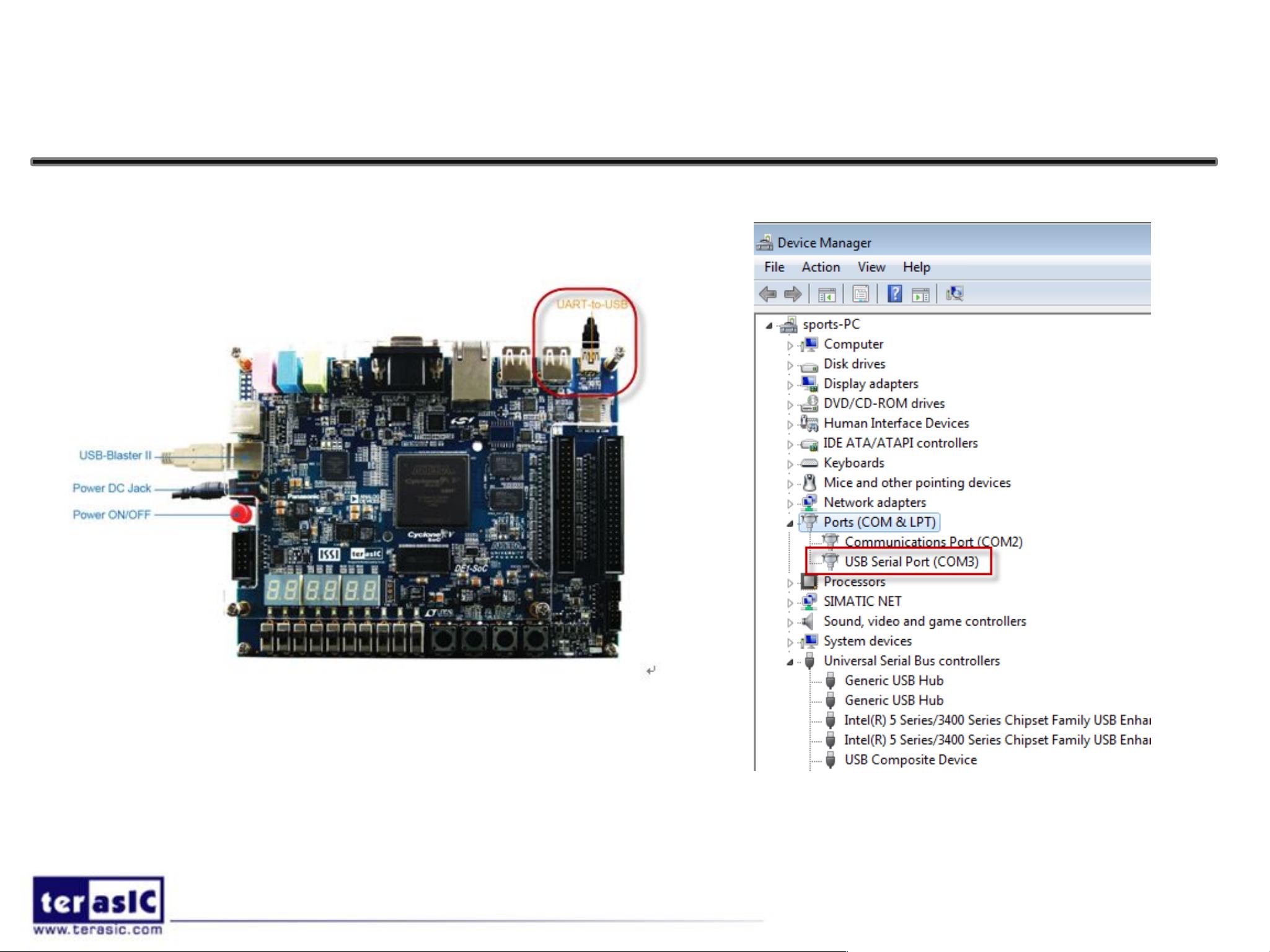
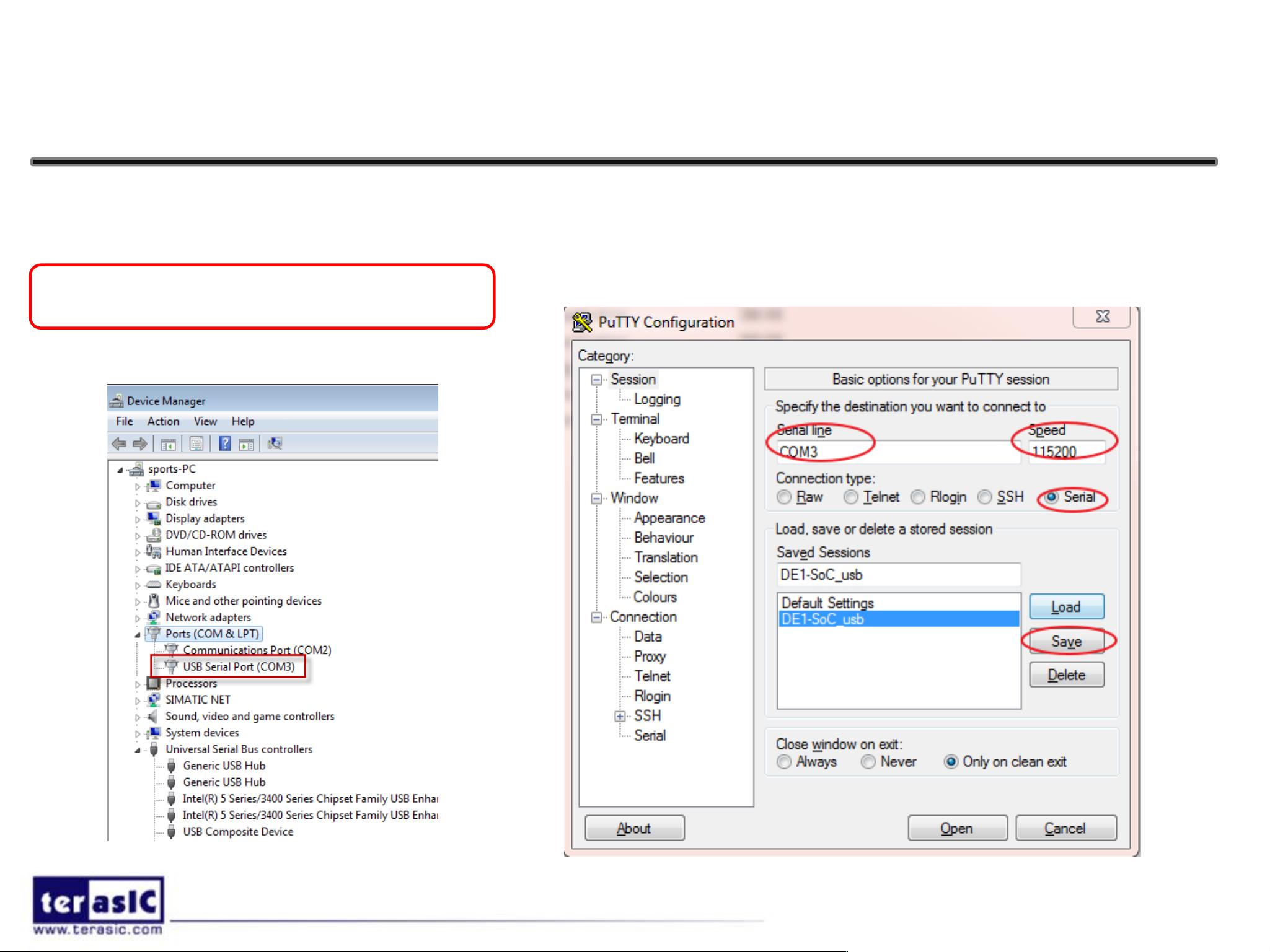
硬件实验部分,重点介绍了DE1-SoC的硬件配置,如通过MSEL引脚设置不同的工作模式,如FPGA配置来自EPCQ(默认)、FPGA配置由HPS(Hard Processor System)软件控制,如Linux或U-Boot,以及使用SD卡加载图像。此外,还提到了如何使用USB Blaster II进行FPGA代码下载和调试,以及如何通过UART-to-USB接口与DE1-SoC进行串口通信,并配置合适的波特率、线路和连接方式。
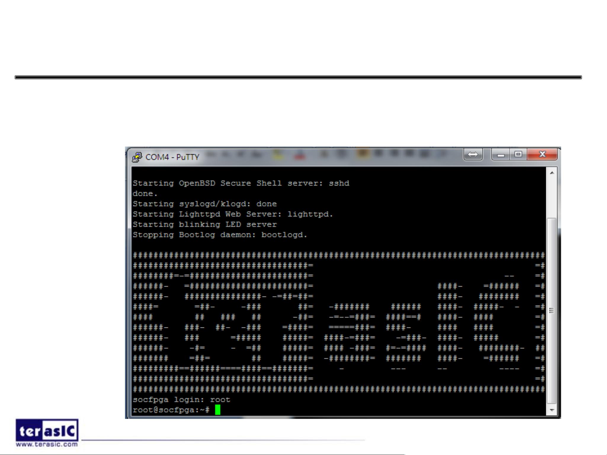
软件实验方面,PPT可能会涉及在DE1-SoC上运行Linux操作系统的过程,包括插入MicroSD卡,以及如何利用这些硬件资源进行实际的系统开发。对于SoCFPGA设计流程,讲解了完整的系统开发流程,包括处理器特性、硬核内存控制器的介绍,这些都是构建高效应用的关键步骤。
整个课程旨在帮助学员掌握ALTERA DE1-SoC开发板的硬件和软件操作,了解其在系统级设计中的角色,并通过实践项目提升实际操作技能。这对于从事嵌入式系统设计、FPGA开发或深入理解SoC架构的工程师来说,是一份实用且深入的培训资料。
2024-05-14 上传
2019-12-13 上传
2014-12-16 上传
2009-01-19 上传
2016-12-01 上传
2017-10-17 上传
2021-11-26 上传
2019-08-04 上传

qq_19400007
- 粉丝: 0
- 资源: 3
 我的内容管理
展开
我的内容管理
展开


最新资源
- Angular实现MarcHayek简历展示应用教程
- Crossbow Spot最新更新 - 获取Chrome扩展新闻
- 量子管道网络优化与Python实现
- Debian系统中APT缓存维护工具的使用方法与实践
- Python模块AccessControl的Windows64位安装文件介绍
- 掌握最新*** Fisher资讯,使用Google Chrome扩展
- Ember应用程序开发流程与环境配置指南
- EZPCOpenSDK_v5.1.2_build***版本更新详情
- Postcode-Finder:利用JavaScript和Google Geocode API实现
- AWS商业交易监控器:航线行为分析与营销策略制定
- AccessControl-4.0b6压缩包详细使用教程
- Python编程实践与技巧汇总
- 使用Sikuli和Python打造颜色求解器项目
- .Net基础视频教程:掌握GDI绘图技术
- 深入理解数据结构与JavaScript实践项目
- 双子座在线裁判系统:提高编程竞赛效率
