Technical Article
MS-2022
.
www.analog.com
May 2011 | Page 1 of 5 ©2011 Analog Devices, Inc. All rights reserved.
Seven Steps to Successful
Analog-to-Digital Signal
Conversion (Noise Calculation
for Proper Signal Conditioning)
by Reza Moghimi, Applications Engineering Manager,
Analog Devices, Inc.
0BIDEA IN BRIEF
High precision applications require a well-designed low
noise analog front end to get the best SNR, which requires
an informed approach to choosing an ADC to fully and
accurately capture sensor signals. Support components
such as driver op amps and references are selected to
optimize overall circuit performance.
eal-world signals, such as vibration, temperature,
pressure, and light, require accurate signal
conditioning and signal conversion before further
data processing in the digital domain. In order to
overcome many challenges in today’s high precision
applications, a well-designed low noise analog front end is
needed to get the best SNR. Many systems cannot afford the
most expensive parts, nor can they afford the higher power
consumption of low noise parts. This article addresses
questions about designing a total solution using a noise-
optimized approach. This article presents a methodical
approach to the design of a gain block and ADC
combination, including an example that supports this
approach. Noise calculation and analysis is performed on
this circuit when conditioning low frequency (near dc)
signals.
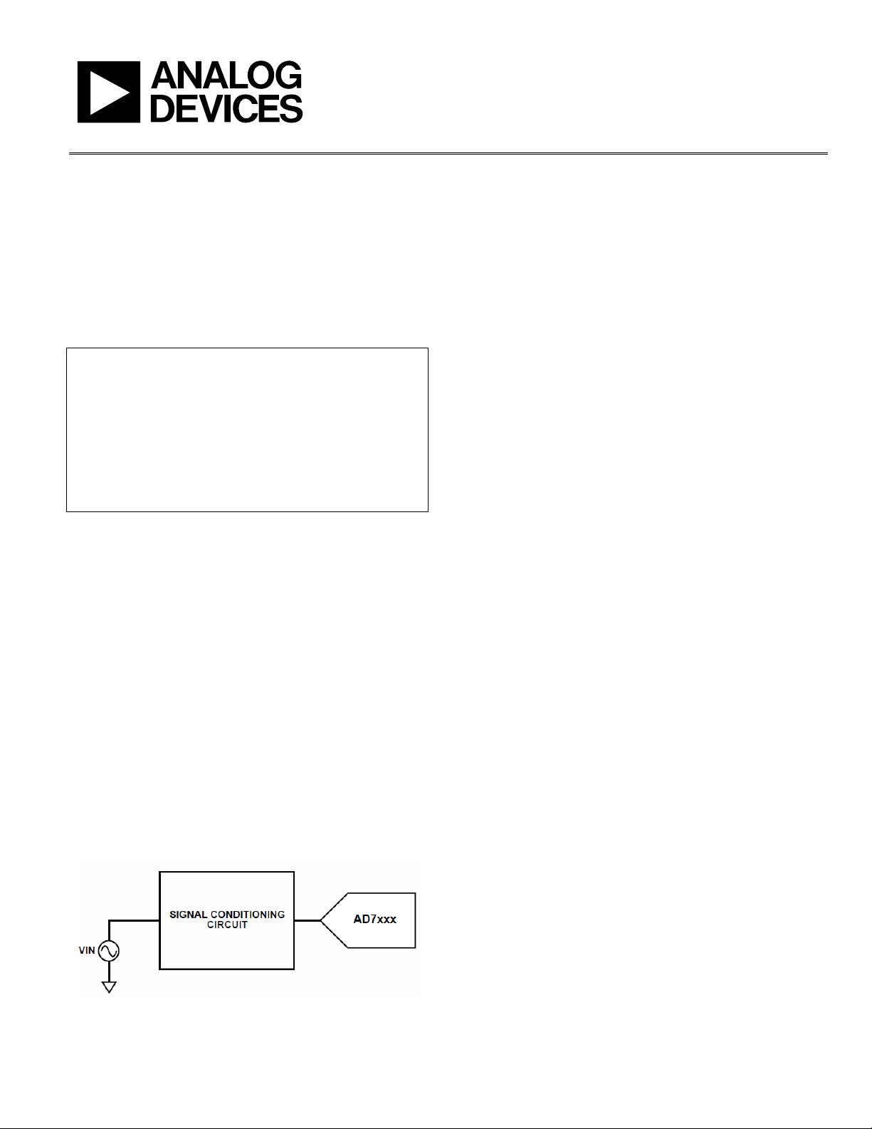
Figure 1. Typical signal conditioning chain.
Follow these seven steps when designing an analog front
end:
1) Describe the electrical output of the sensor or section
preceding the gain block.
2) Calculate the ADC’s requirements.
3) Find the optimal ADC + voltage reference for the signal
conversion.
4) Find the maximum gain and define search criteria for
the op amp.
5) Find the optimal amplifier and design the gain block.
6) Check the total solution noise against the design target.
7) Run simulation and validate.
Step 1: Describe the electrical output of the sensor or
section preceding the gain block
Signals can come directly from the sensor or may have gone
through EMI and RFI filters prior to the gain block. In order
to design the gain block, one needs to know the ac and dc
characteristics of the signal and the available power supplies.
Knowing the signal’s characteristic and noise level provides
clues as to what input voltage range and noise levels we
might need when selecting an ADC. Let’s assume that we
have a sensor that outputs a 10 kHz signal with full-scale
amplitude of 250 mV p-p (88.2 mV rms) and 25 μV p-p
noise. Let’s additionally assume that we have a 5 V supply
available in our system. With this information we should be
able to calculate the signal-to-noise ratio at the ADC’s input
in step 2. To simplify data crunching and confusion, assume
that we design this solution for room temperature operation.
Step 2: Calculate the ADC’s requirement
What type of ADC, what sample rate, how many bits, and
what noise specification do we need? By knowing the input
signal amplitude and noise information from step 1, we can
calculate the signal-to-noise ratio (SNR) at the gain block’s
input. We need to pick an ADC that has better signal-to-
noise ratio. Knowing the SNR will help us to calculate the
effective number of bits (ENOB) when choosing the ADC.
This relationship is shown in the following equations. Both
SNR and ENOB are always specified in any good ADC
data sheet. In this example, the required 86.8 dB SNR and
14.2-bit ENOB force us to choose a 16-bit analog-to-digital
converter. Additionally the Nyquist criterion states that the
sampling rate, fs, should be at least twice the maximum
incoming frequency, fin, so a 20 kSPS ADC would suffice.


