Analog Applications Journal
High-Performance Analog Products www.ti.com/aaj 4Q 2012
Texas Instruments Incorporated
14
LDO noise examined in detail
Introduction
Requirements and expectations for telecommuni-
cation systems continue to evolve as complexity
and reliability of the communication channels
continue to increase. These communication sys-
tems rely heavily on high-performance, high-speed
clocking and data-converter devices. The perform-
ance of these devices is highly dependent on the
quality of system power rails. A clock or converter
IC simply cannot achieve top perform ance when
powered by a dirty power supply. Just a small
amount of noise on the power supply can cause
dramatic negative effects on the perform ance.
This article examines a basic LDO topology to find
its dominant noise sources and suggests ways to
minimize its output noise.
A key parameter indicating the quality of a
power supply is its noise output, which is com-
monly referred by the RMS noise measurement or
by the spectral noise density. For the lowest RMS
noise or the best spectral noise characteristics, a
linear voltage regulator like a low-dropout voltage
regulator (LDO) always has an advantage over a
switching regulator. This makes it the power sup-
ply of choice for noise-critical applications.
Basic LDO topology
A simple linear voltage regulator consists of a
basic control loop where a negative feedback is
compared to an internal reference in order to pro-
vide a constant voltage—regardless of changes or
perturbations in the input voltage, temperature, or
load current.
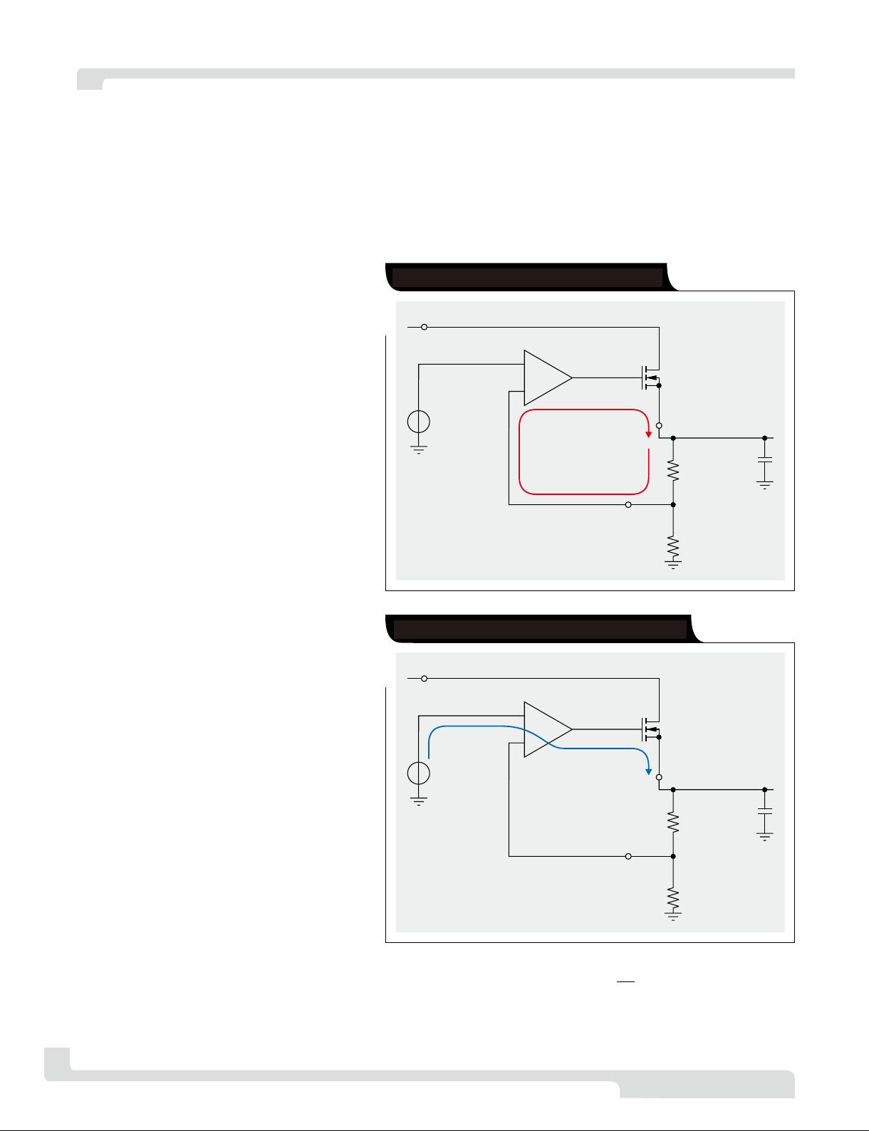
Figure 1 shows a basic block diagram of an LDO
regulator. The red arrow indicates the negative-
feedback signal path. The output voltage, V
OUT
, is
divided by feedback resistors R1 and R2 to provide
the feedback voltage, V
FB
. V
FB
is compared to the
reference voltage, V
REF
, at the negative input of
the error amplifier to supply the gate-drive voltage,
V
GATE
. Finally, the error signal drives the output
transistor, NFET, to regulate V
OUT
.
A simplified analysis of noise begins with Figure 2.
The blue arrow traces a subset of the loop repre-
sented by a common amplifier variation known as a volt-
age follower or power buffer. This voltage-follower circuit
forces V
OUT
to follow V
REF
. V
FB
is the error signal referring
to V
REF
. In steady state, V
OUT
is bigger than V
REF
, as
described in Equation 1:
By Masashi Nogawa
Senior Systems Engineer, Linear Regulators
Power Management
V
IN
C
OUT
R1
R2
V
REF
V
GATE
+
–
+
–
NFET
OUT Node
(
V
)
OUT
FB Node
(
V
)
FB
Error
Amp
Figure 1. Negative-feedback loop of LDO
OUT REF
R1
V 1 V ,
R2
=+ ×
(1)
where 1 + R1/R2 is the gain that the error amplifier must
have to obtain the steady-state output voltage (V
OUT
).
V
IN
C
OUT
R1
R2
V
REF
V
GATE
+
–
+
–
NFET
OUT Node
(
V
)
OUT
FB Node
(
V
)
FB
Error
Amp
Figure 2. Reference-voltage buffering of LDO


