INA226电流电压监测器:精准测量,I2C接口
需积分: 5 49 浏览量
更新于2024-06-18
2
收藏 1.21MB PDF 举报
"INA226中文手册自译,高低端电流检测IC,电流电压测量芯片"
INA226是一款高性能的电流和电压检测集成电路,专为监控电子设备的电源管理和能耗而设计。这款芯片能够精确地测量从0到36伏的总线电压,并且可以在高端或低端进行电流检测,不受电源电压的影响。它采用了I2C或SMBUS兼容的接口,允许用户通过微控制器或其他控制设备轻松地读取和设置参数。
INA226的关键特性包括:
1. 总线电压检测:INA226可以监测0至36伏的总线电压,这使得它适用于各种电源系统,如服务器、电信设备、电池充电器等。
2. 电流检测:无论是高侧(高端)还是低侧(低端)检测,INA226都能提供精确的电流测量。它能处理共模总线电压上的电流变化,无需考虑电源电压。
3. 精度保证:INA226具有卓越的精度,增益误差最大仅为0.1%,失调电压最大为10微伏,确保了测量结果的可靠性。
4. 可配置性:用户可以根据需求配置校准值、转换时间和均值选项,从而适应不同的应用环境。
5. 16个可编程地址:通过I2C兼容接口,INA226支持多达16个不同的地址,便于在同一系统中集成多个传感器。
6. 低功耗:使用2.7至5.5伏的单电源供电,典型功耗只有330微安,适合能源敏感的应用。
7. 封装形式:INA226采用10引脚的VSSOP封装,尺寸为3.00mm x 3.00mm,便于安装在紧凑的电路板上。
8. 工作温度范围:芯片的工作温度范围为-40°C至125°C,确保在恶劣环境下也能稳定工作。
在实际应用中,INA226可以用于实时监控系统的电源状态,比如计算设备的功耗、电池充电状态的监测、电力供应的故障诊断以及测试设备的性能评估。通过I2C兼容接口,用户可以轻松地获取电流、电压和功率的数据,并根据这些信息做出相应的控制决策。
总结来说,INA226是一款功能强大、精度高、可配置性强的电流和电压测量芯片,广泛应用于需要精确电源管理和能耗监控的领域。其独特的设计和优秀的性能指标使其成为电源监控解决方案的理想选择。
Population
-100
-80
-60
-40
-20
0
20
40
60
80
100
Input Gain Error (m%)
0
100
200
300
400
500
600
−50 −25 0 25 50 75 100 125
Temperature (°C)
Gain Error (m%)
G007
−2.4
−2.2
−2
−1.8
−1.6
−1.4
−1.2
−1
−50 −25 0 25 50 75 100 125
Temperature (°C)
Offset (µV)
G003
140
150
160
170
−50 −25 0 25 50 75 100 125
Temperature (°C)
Common−Mode Rejection Ratio (dB)
G004
Population
-10
-8
-6
-4
-2
0
2
4
6
8
10
Input Offset Voltage ( V)m
−60
−50
−40
−30
−20
−10
0
1 10 100 1k 10k 100k
Frequency (Hz)
Gain (dB)
G001
INA226
www.ti.com
SBOS547A –JUNE 2011–REVISED AUGUST 2015
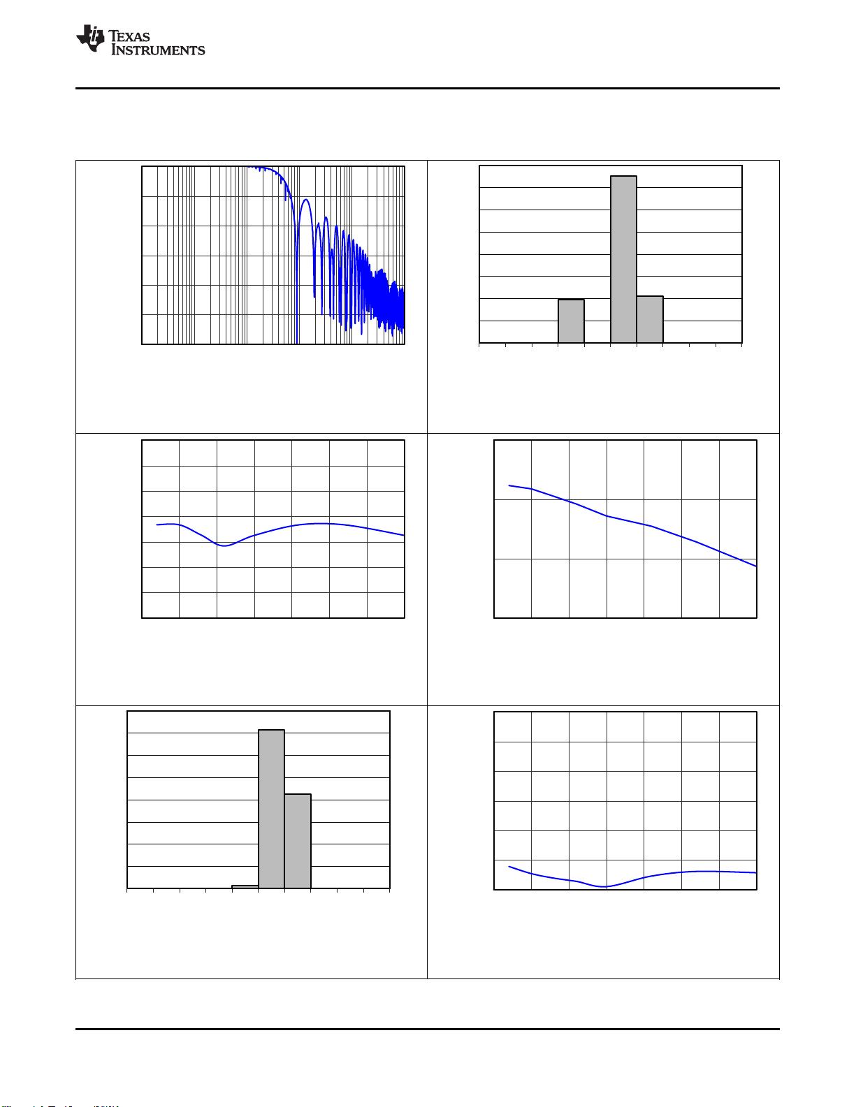
6.6 Typical Characteristics
At T
A
= 25°C, V
VS
= 3.3 V, V
IN+
= 12 V, V
SENSE
= (V
IN+
– V
IN–
) = 0 mV and V
VBUS
= 12 V, unless otherwise noted.
Figure 2. Shunt Input Offset Voltage Production Distribution
Figure 1. Frequency Response
Figure 3. Shunt Input Offset Voltage vs Temperature Figure 4. Shunt Input Common-Mode Rejection Ratio vs
Temperature
Figure 5. Shunt Input Gain Error Production Distribution
Figure 6. Shunt Input Gain Error vs Temperature
Copyright © 2011–2015, Texas Instruments Incorporated Submit Documentation Feedback 7
Product Folder Links: INA226

剩余38页未读,继续阅读
2950 浏览量
3542 浏览量
352 浏览量
3542 浏览量
5782 浏览量
480 浏览量
4709 浏览量

qq9650886
- 粉丝: 1
 我的内容管理
展开
我的内容管理
展开


最新资源
- 流浪汉环境性能比较:Virtualbox vs Parallels
- WatchMe项目使用TypeScript进行开发的介绍
- Nali:全面支持IPv4/IPv6离线查询IP地理及CDN信息工具
- 利用pdfjs-2.2.228-dist实现零插件PDF在线预览技术
- MATLAB与jEdit集成:实用工具包发布
- Vagrant、Ansible和Docker搭建Django应用环境
- 使用Delphi更改计算机名称的详细教程
- TrueNAS CORE中iocage-homeassistant插件的高级安装方法
- rack程序:命令行工具高效处理天气雷达数据
- VS2017下实现C# TCP一对多通信程序源码
- MATLAB项目管理器:快速切换与路径管理
- LightDM GTK+ Greeter设置编辑器的Python图形界面介绍
- 掌握CSS技巧,提升网页设计美感
- 一维RCWA算法在matlab中的实现与应用
- Hot Reload插件:提升Flutter开发效率的Vim工具
- 全面掌握Dubbo:Java面试题及详细答案解析
