908 IEEE TRANSACTIONS ON COMPONENTS, PACKAGING AND MANUFACTURING TECHNOLOGY, VOL. 6, NO. 6, JUNE 2016
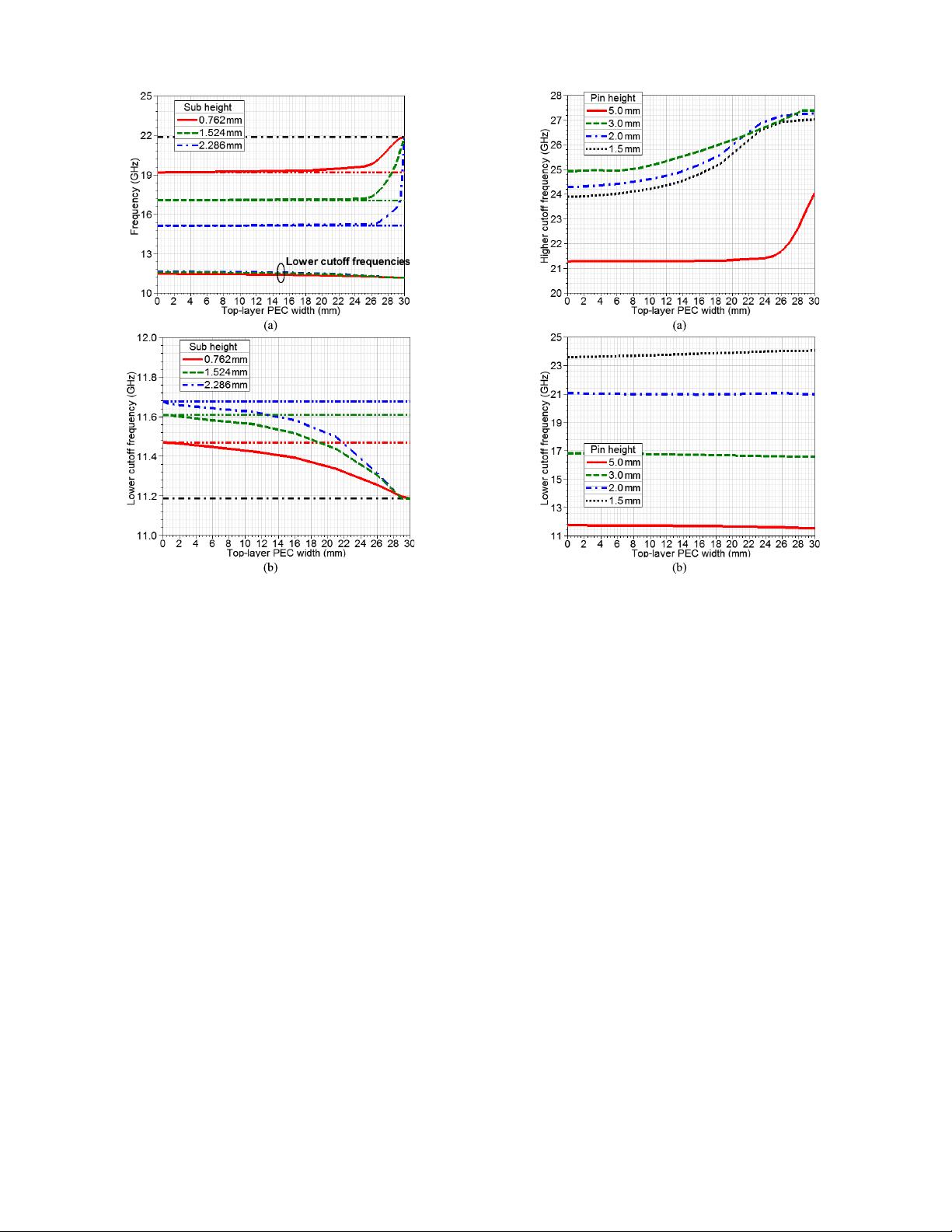
Fig. 3. Change in stopband with top-layer PEC width at three different
substrate heights. (a) Lower and higher cutoff frequencies. (b) Zoomed-in
view of lower cutoff frequencies. A square-shaped pin with a size of 3.0 mm
is used.
pin height is smaller than 2.0 mm, the higher cutoff frequency
even rises immediately as far as the width of the top PEC
surface is larger than zero. This is very different from the
substrate height effect presented in Figs. 2 and 3. The lower
cutoff frequencies, however, are quite different for different
pin heights, but the top PEC surface width impact is negligible
as shown in Fig. 4(b), similar to Figs. 2 and 3 for different
substrate heights.
Further, Fig. 5(a) reveals that a larger air gap height reduces
the higher cutoff frequencies and makes the higher cutoff more
sensitive to the top-layer PEC width. The evidence is that for
an air gap of 2.0 mm, the higher cutoff frequency starts rising
at a narrower top-layer PEC width, compared with the air gap
of 0.5- and 1.0-mm height. This is opposite for the lower cutoff
seen in Fig. 5(b). For example, for a smaller air gap height
of 0.5 mm, a larger drop range of the lower cutoff frequencies
is presented with increased top-layer PEC width. Even so,
the total variation range of the lower cutoff frequencies is still
very small in comparison with that of the higher cutoff.
C. Number of Metal Pin Columns
The study of a GW including two-layer PEC surfaces should
consider different PMC configurations; thus, in this part,
two more PMC lids of pins are built, which employ six-
and seven-column pins. Moreover, this is also needed for
a large circuit or other purposes where more pins are required.
Fig. 4. Change in stopband with top-layer PEC width at four different pin
heights. (a) Higher cutoff frequencies. (b) Lower cutoff frequencies.
The pins of the built PMC lids have the same dimensions
as given above: pin size of 1.5 mm, pin height of 5.0 mm,
air gap height of 1.0 mm, and cell period of 6.0 mm. The
total width (W) is increased from 30 mm to 36 and 42 mm,
respectively, due to the increased pin columns of six and
seven. The adopted substrate is Rogers RT/Duroid 6002 with
ε
r
of 2.94 and height of 0.762 mm.
The simulated results for the built lids of pins with different
columns are presented in Fig. 6. It can be seen that the created
higher cutoff frequencies have the same minimum value for
five-, six-, and seven-column pins. Although the three higher
cutoff curves rise at different top-layer PEC widths, they all
happen when the PEC width extends so big that the substrate
has a width of only one cell period of 6.0 mm. Fig. 6(b) then
shows that the three generated lower cutoff frequencies have
a small decline with the top-layer PEC width. And they all
drop down once the PEC width is larger than zero and arrive
at the minimum value when the top PEC surface width is
equal to the total width (W). But for a particular top-layer PEC
width, such as 21 mm, the PMC lid with more columns of pins
apparently hinders the decline of the lower cutoff frequencies.
D. Substrates With Different Permittivities
The last factor considered in the cell-based analysis of the
two-layer PEC surfaces is the dielectric substrate permittivity,
since the uncovered substrate is exposed to PMC shielding
and thus its permittivity will affect the created stopband [21].


