TI电源管理芯片解析:线性稳压器与开关模式
需积分: 14 194 浏览量
更新于2024-07-18
1
收藏 2.56MB PDF 举报
"TI电源管理芯片包括线性稳压器如TPS7xxx系列和开关模式稳压器,如电感型和电荷泵。线性稳压器工作原理是通过调整管(通常是MOSFET)来维持输出电压稳定,但效率较低,因为能量消耗在调整管上。现代LDO利用MOSFET的小RDSON实现更低的电压降。在选择线性稳压器时,需关注VOUT精度、VIN范围、VDO与IOUT的关系、热特性、静态电流IQ、电源纹波抑制比和噪声密度等关键参数。效率可近似通过Vout/Vin计算,而功率耗散为(Vin-Vout)×Iout。"
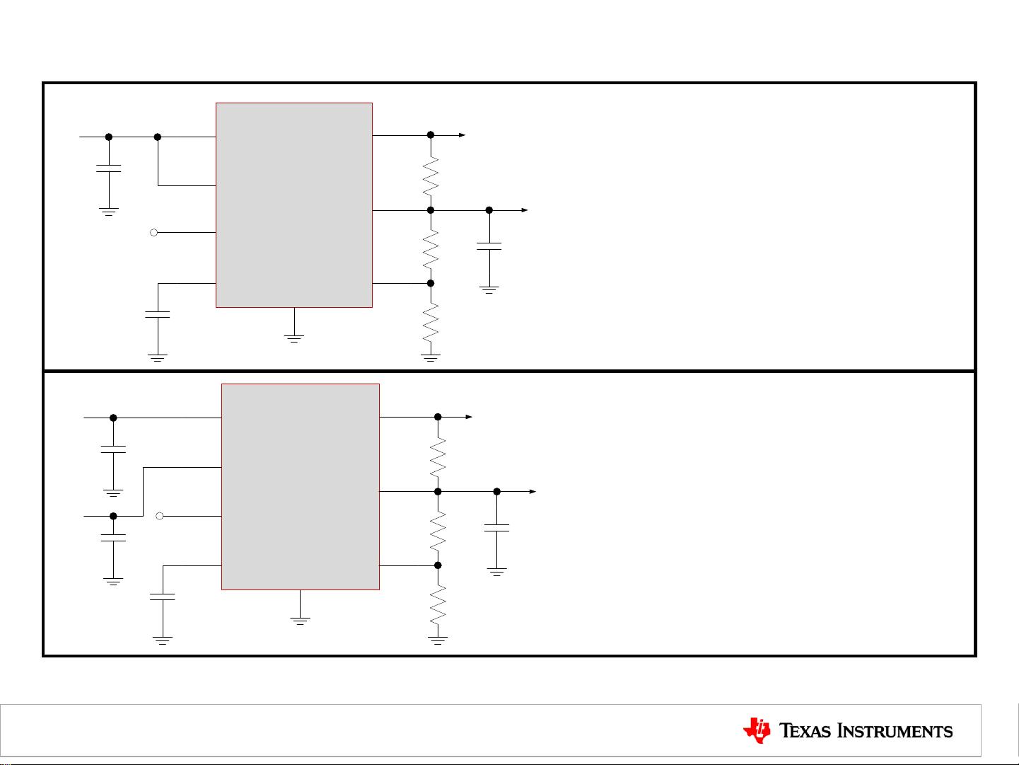
TI公司的电源管理芯片提供多种类型的解决方案,其中线性稳压器如TPS7xxx系列是常见的一种。线性稳压器保持输出电压恒定,其工作原理是通过一个内部调整管(通常为MOSFET)改变其阻抗来调节输出电压。尽管简单且输出电压稳定,但因为输入电压必须大于输出电压,所以当两者差距较大时,效率降低,能量以热量形式损耗。
线性稳压器的核心组件包括误差放大器、参考电压VREF、以及通路晶体管。误差放大器比较输出电压VOUT与内部参考电压,并调整通路晶体管以维持VOUT的稳定。现代线性稳压器,特别是LDO(低压差稳压器),利用MOSFET的低电阻特性,能在输入输出电压差极小的情况下仍保持高效运行。
在选择线性稳压器时,有多个关键参数需要考虑。VOUT精度是衡量输出电压准确度的重要指标,TI公司规定了全温度范围内的VOUT精度。VIN范围则影响稳压器在不同输入电压下的性能,低输入电压可能会导致性能下降。VDO(电压差)是指输入电压与输出电压之间的最小差值,它与负载电流IOUT有关。热特性至关重要,确保封装能承受预期环境下的功率损耗。静态电流IQ在负载电流非常小时显得尤为重要,因为它即使在无负载时也会消耗电力。此外,电源纹波抑制比(PSRR)衡量了稳压器对输入电源噪声的抑制能力,而噪声密度则反映了输出电压的噪声水平。
在效率方面,线性稳压器的效率通常低于开关模式稳压器,因为它不涉及能量转换,而是通过调整管直接消耗输入电压的一部分。忽略静态电流,效率大约等于Vout/Vin。然而,实际的功率耗散(PD)等于输入电压与输出电压差与负载电流的乘积,即PD=(Vin-Vout)×Iout。
TI的电源管理芯片涵盖了各种电源解决方案,而线性稳压器因其稳定性和易用性在许多应用中被广泛采用。选择合适的线性稳压器需要综合考虑上述各项技术参数,以确保在特定应用环境下达到最佳性能和效率。
例如V
BIAS
> V
IN
V
IN
– 1.5V
V
OUT
– 1.2V
V
BIAS
> 3V
Eff = P
OUT
/ P
IN
~ V
OUT
/ V
IN
Eff = 1.2/1.5 x 100 = 80%
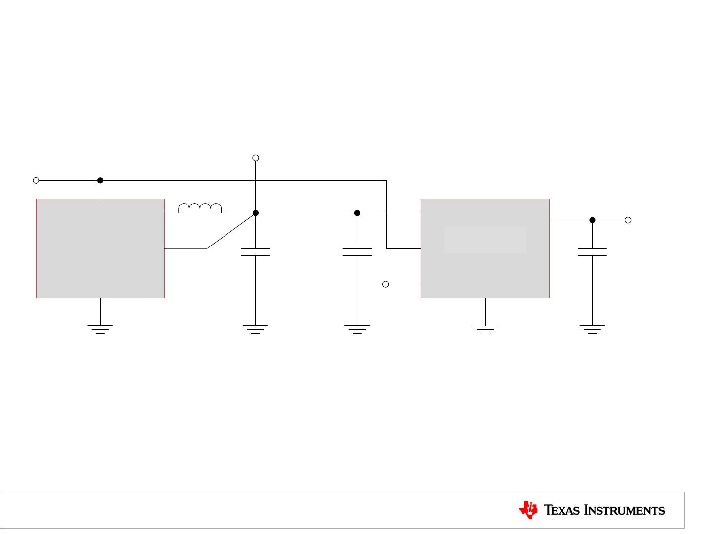
V
BIAS
– 增加LDO 性能
例如V
BIAS
= V
IN
V
IN
– 3.3V
V
OUT
– 1.2V
V
BIAS
– 3.3V
Eff = P
OUT
/ P
IN
~ V
OUT
/ V
IN
Eff = 1.2/3.3 x 100 = 36%
V
IN
V
BIAS
Enbable
Soft
Start
Power
Good
V
OUT
Feed
Back
GND
C
IN
C
BIAS
C
SS
C
OUT
1.2V @500mA
1.5V
V
BIAS
> 3V
TPS74701
1.2V @500mA
V
IN
V
BIAS
Enbable
Soft
Start
Power
Good
V
OUT
Feed
Back
GND
C
IN
C
SS
C
OUT
3.3V
TPS74701


剩余102页未读,继续阅读
2019-06-24 上传
261 浏览量
2021-01-19 上传
2020-12-01 上传
2020-11-21 上传
点击了解资源详情

zq113
- 粉丝: 0
- 资源: 8
 我的内容管理
展开
我的内容管理
展开


最新资源
- 新型智能电加热器:触摸感应与自动温控技术
- 社区物流信息管理系统的毕业设计实现
- VB门诊管理系统设计与实现(附论文与源代码)
- 剪叉式高空作业平台稳定性研究与创新设计
- DAMA CDGA考试必备:真题模拟及章节重点解析
- TaskExplorer:全新升级的系统监控与任务管理工具
- 新型碎纸机进纸间隙调整技术解析
- 有腿移动机器人动作教学与技术存储介质的研究
- 基于遗传算法优化的RBF神经网络分析工具
- Visual Basic入门教程完整版PDF下载
- 海洋岸滩保洁与垃圾清运服务招标文件公示
- 触摸屏测量仪器与粘度测定方法
- PSO多目标优化问题求解代码详解
- 有机硅组合物及差异剥离纸或膜技术分析
- Win10快速关机技巧:去除关机阻止功能
- 创新打印机设计:速释打印头与压纸辊安装拆卸便捷性
