1856 IEEE PHOTONICS TECHNOLOGY LETTERS, VOL. 29, NO. 21, NOVEMBER 1, 2017
Study of LED Thermal Resistance and TIM
Evaluation Using LEDs With Built-in Sensor
Xiaoli Wang, Yugang Zhou, Renbao Tian, Bin Liu, Zili Xie, Rong Zhang, and Youdou Zheng
Abstract—This study developed an LED thermal resistance
and thermal interface material evaluation method using LEDs
with an internal sensor unit by both steady-state and transient
thermal measurements. The problem of the measurement delay
time caused by the current switching, which exist in conventional
methods can be avoided in both steady-state and transient
thermal measurements. Slight error in junction temperature mea-
surement caused by the self-illumination effect can be identified
without the current switching issue. The error is compensated in
steady-state thermal measurement and is insignificant in transient
measurement. Compared with conventional methods, this method
uses low-cost equipment, while realizing improved accuracy.
Index Terms— Junction temperature, thermal resistance, light
emitting diode, thermal interface materials.
I. INTRODUCTION
L
IGHT emitting diodes (LEDs) have become a new
generation of solid-state lighting sources due to their
advantages of long lifetime, low power consumption, short
response time, and environmental friendliness [1]. Junction
temperature and thermal resistance are critical to character-
ize the thermal performance of LED products [2]. Thermal
interface materials (TIM) are one of the most critical factors
for thermal performance and reliability of the LED package.
A fast and accurate junction temperature (T
j
) measurement
method contributes to the judgement of TIM performance.
The forward voltage method is commonly applied for T
j
measurements [3]–[5]. Using the conventional forward voltage
method, the forward current will switch between working
current and small measurement current. Measurement delay
time (t
MD
) must be considered for two reasons: either the test
system cannot switch fast enough to ensure accurate voltage
measurement, or the device cannot switch fast enough due
to excessive capacitance or other circuit problems [5]. With
non-zero t
MD
, the junction cooling or heating after switching
will cause measurement errors. This means that expensive and
complicated equipment is required to enable fast switching
Manuscript received June 29, 2017; revised August 26, 2017; accepted
September 11, 2017. Date of publication September 18, 2017; date of current
version October 13, 2017. This work was supported in part by the National
Natural Science Foundation of China under Grant 61334009 and Grant
61634005, in part by the National Key Research and Development Program of
China under Grant 2016YFB0400904, in part by the Collaborative Innovation
Center of Solid-State Lighting and Energy-Saving Electronics and in part by
the Project Funded by the Priority Academic Program Development of Jiangsu
Higher Education Institutions. (Corresponding author: Yugang Zhou.)
The authors are with the Jiangsu Provincial Key Laboratory of Advanced
Photonic and Electronic Materials, School of Electronic Science and Engineer-
ing, Nanjing University, Nanjing 210023, China (e-mail: ygzhou@nju.edu.cn).
Color versions of one or more of the figures in this letter are available
online at http://ieeexplore.ieee.org.
Digital Object Identifier 10.1109/LPT.2017.2753942
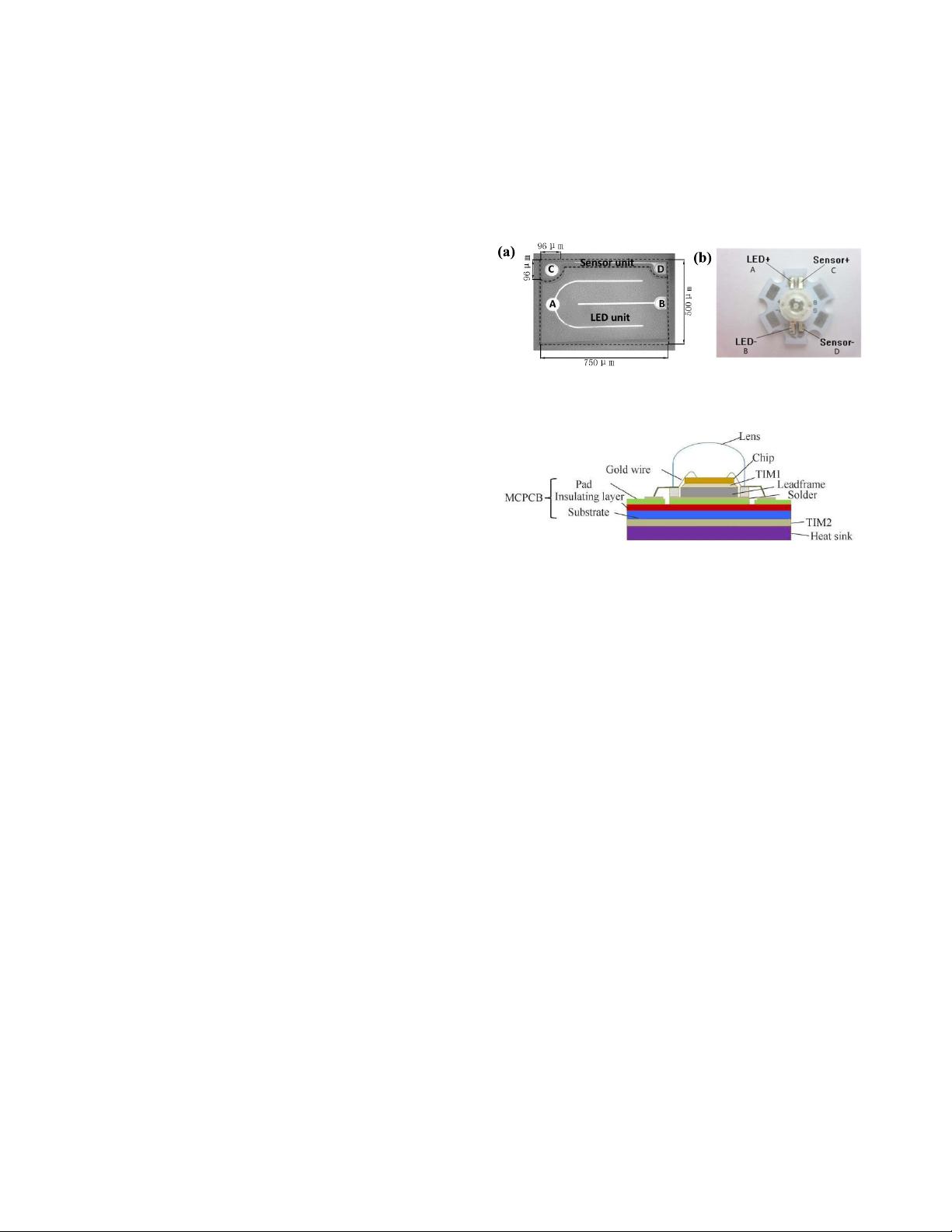
Fig. 1. (a). bare-chip photograph of LED chip with internal sensor;
(b) the photograph of the LED package mounted on MCPCB.
Fig. 2. The structure of LED samples with TIM.
and smaller t
MD
for precise measurement of transient T
j
and
further analysis of structure function of LED and evaluation
of TIM.
In a previous study, we proposed a novel LED structure with
an internal sensor unit for T
j
measurement without current
switching [6]. For this letter, we further studied the evaluation
of thermal interface material and LED thermal properties using
this novel LED structure. Both the junction-to-ambient steady
thermal resistance and transient thermal impedance of LEDs
with different TIM were studied.
II. E
XPERIMENTAL DETAILS
Blue LED chips with an internal sensor unit were used
in this study, and the chip structure has previously been
described [6]. Isolated LED unit and sensor unit were inte-
grated into a single chip, as is shown in Fig. 1(a). The whole
chip size is 750 × 500 μm
2
. The effective light-emission
area of the LED unit is around 750 × 430 μm
2
and the
effective p-n junction area of the sensor unit is around
96 × 96 μm
2
. The chips were packaged using a four-lead
high-power leadframe, then the packages were mounted on
a metal-core printed circuit board (MCPCB), as is shown in
Fig. 1(b). Fig. 2 shows the thermal dissipation structure of
LED samples shown in Fig.1(b). The forward voltage of the
sensor diode was used to characterize the junction temperature
after calibration.
Three parts of the experiments were performed. The first
measured the transient T
j
, using the internal sensor and
1041-1135 © 2017 IEEE. Personal use is permitted, but republication/redistribution requires IEEE permission.
See http://www.ieee.org/publications_standards/publications/rights/index.html for more information.


