Pin Descriptions
Table 1: SPI Pin Descriptions
Symbol Type Description
CS# Input Chip select: Places the device in active power mode when driven LOW. Deselects the de-
vice and places SO at High-Z when HIGH. After power-up, the device requires a falling
edge on CS# before any command can be written.
The device goes into standby mode when no PROGRAM, ERASE, or WRITE STATUS REGIS-
TER operation is in progress.
In the case of write-type instructions, CS# must be driven HIGH after a whole sequence is
completed. Single command and address sequences and array-based operations are regis-
tered on CS#.
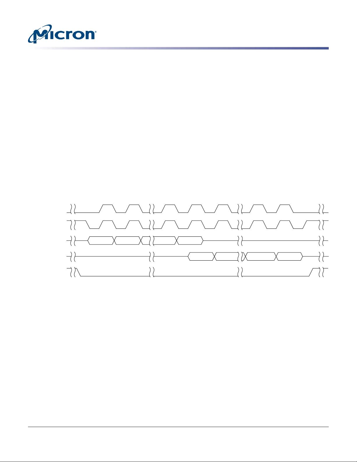
SCK Input Serial clock: Provides serial interface timing. Latches commands, addresses, and data on
SI on the rising edge of SCK. Triggers output on SO after the falling edge of SCK. While
CS# is HIGH, keep SCK at V
CC
or GND (determined by mode 0 or mode 3). Do not toggle
SCK until CS# is driven LOW.
WP# Input Write protect: When LOW, prevents overwriting block lock bits (BP[3:0] and TB) if the
block register write disable (BRWD) bit is set.
WP# must not be driven by the host during a x4 READ operation. If the device is deselec-
ted, this pin defaults as an input pin.
HOLD# Input Hold: Hold functionality is disabled by default except the special part numbers. Contact
Micron Sales representatives for details. When enabled, the external pull-up resistor is
necessary to avoid accidental operation being placed on hold.
HOLD# pauses any serial communication with the device without deselecting it. To start
the HOLD condition, the device must be selected, with CS# driven LOW. During HOLD sta-
tus (HOLD# driven LOW), SO is High-Z and all inputs at SI and SCK are ignored. Hold
mode starts at the falling edge of HOLD#, provided SCK is also LOW. If SCK is HIGH when
HOLD# goes LOW, hold mode is kicked off at the next falling edge of SCK. Similarly, hold
mode is exited at the rising edge of HOLD#, provided SCK is also LOW. If SCK is HIGH,
hold mode ends after the next falling edge of SCK. HOLD# must not be driven by the host
during the x4 READ operation.
SI/IO0, SO/IO1,
IO2, IO3
I/O Serial I/O: The bidirectional I/O signals transfer address, data, and command information.
The device latches commands, addresses, and data on the rising edge of SCK, and data is
shifted out on the falling edge of the SCK. If the device is deselected, IO[0,2] defaults as
an input pin and IO[1,3] defaults as an output pin.
SI must not be driven by the host during x2 or x4 READ operations.
V
CC
Supply V
CC
: Supply voltage
V
SS
Supply V
SS
: Ground
DNU – Do not use: Must be left floating.
NC – No Connect: Not internal connection; can be driven or floated.
Micron Confidential and Proprietary
4Gb 3.3V x1, x2, x4: SPI NAND Flash Memory
Pin Descriptions
X26P4QTWDSPK-13-10136
m79a_DDP_nand_spi_4gb_3v.pdf – Rev. G 04/17 EN
10
Micron Technology, Inc. reserves the right to change products or specifications without notice.
© 2015 Micron Technology, Inc. All rights reserved.


