
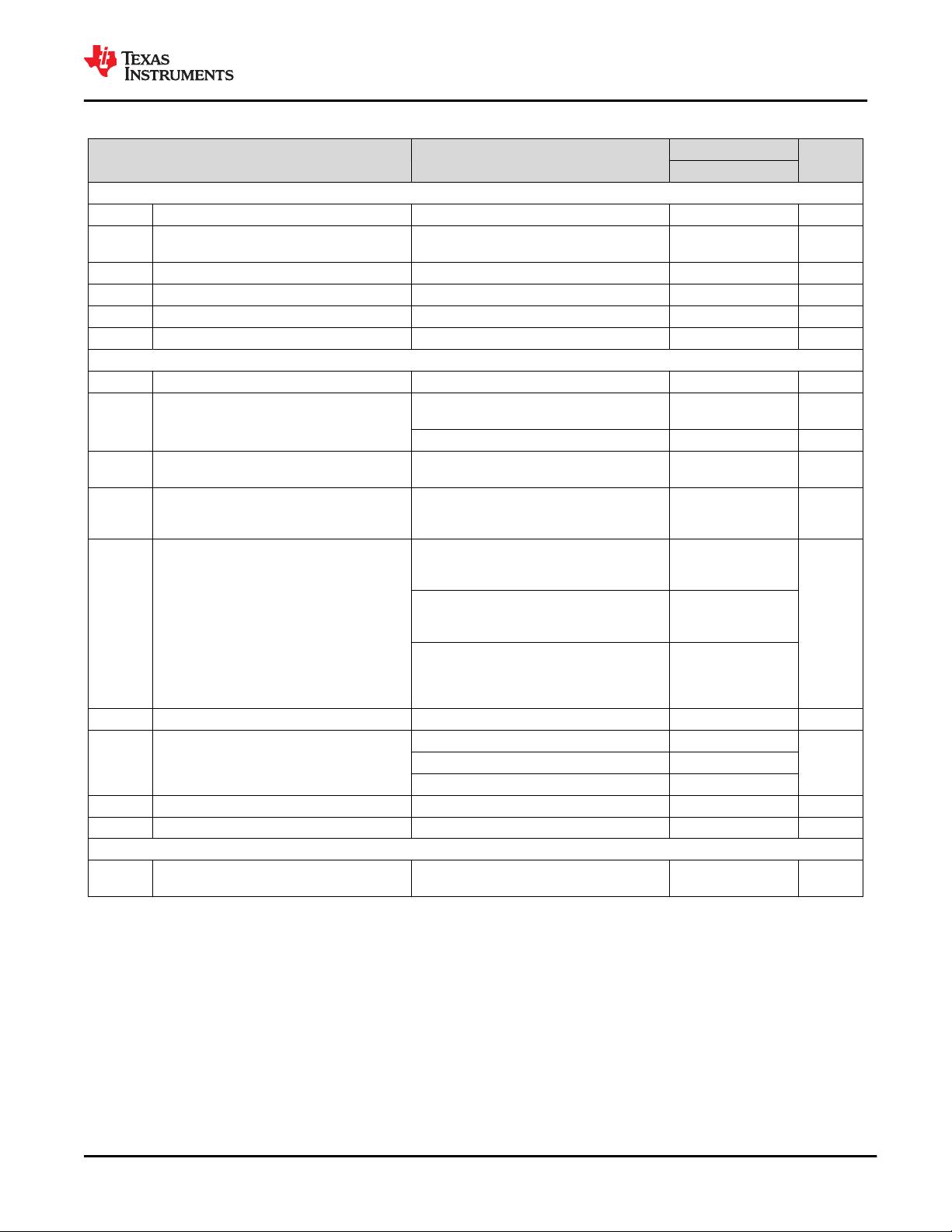
Insulation Specifications
PARAMETER TEST CONDITIONS
SPECIFICATIONS
UNIT
QSOP-16
IEC 60664-1
CLR External clearance
(1)
Side 1 to side 2 distance through air >3.7 mm
CPG External Creepage
(1)
Side 1 to side 2 distance across package
surface
>3.7 mm
DTI Distance through the insulation Minimum internal gap (internal clearance) 17 µm
CTI Comparative tracking index IEC 60112; UL 746A >600 V
Material Group According to IEC 60664-1 I
Overvoltage category per IEC 60664-1 Rated mains voltage ≤ 300 V
RMS
I-III
DIN V VDE V 0884-11:2017-01
(2)
V
IORM
Maximum repetitive peak isolation voltage AC voltage (bipolar) 566 V
PK
V
IOWM
Maximum isolation working voltage
AC voltage (sine wave); time-dependent
dielectric breakdown (TDDB) test; See TBD
400 V
RMS
DC voltage 566 V
DC
V
IOTM
Maximum transient isolation voltage
V
TEST
= V
IOTM
, t = 60 s (qualification); V
TEST
= 1.2 × V
IOTM
, t = 1 s (100% production)
4242 V
PK
V
IOSM
Maximum surge isolation voltage
(3)
Test method per IEC 62368-1, 1.2/50 µs
waveform, V
TEST
= 1.6 × V
IOSM
= 6400 V
PK
(qualification)
4000 V
PK
q
pd
Apparent charge
(4)
Method a: After I/O safety test subgroup 2/3,
V
ini
= V
IOTM
, t
ini
= 60 s; V
pd(m)
= 1.2 × V
IORM
,
t
m
= 10 s
≤ 5
pC
Method a: After environmental tests subgroup
1, V
ini
= V
IOTM
, t
ini
= 60 s;
V
pd(m)
= 1.6 × V
IORM
, t
m
= 10 s
≤ 5
Method b1: At routine test (100% production)
and preconditioning (type test), V
ini
= V
IOTM
,
t
ini
= 1 s;
V
pd(m)
= 1.875 × V
IORM
, t
m
= 1 s
≤ 5
C
IO
Barrier capacitance, input to output
(5)
V
IO
= 0.4 × sin (2 πft), f = 1 MHz ~1.5 pF
R
IO
Insulation resistance, input to output
(5)
V
IO
= 500 V, T
A
= 25°C > 10
12
ΩV
IO
= 500 V, 100°C ≤ T
A
≤ 150°C > 10
11
V
IO
= 500 V at T
S
= 150°C > 10
9
Pollution degree 2
Climatic category 55/125/21
UL 1577
V
ISO
Withstand isolation voltage
V
TEST
= V
ISO
, t = 60 s (qualification); V
TEST
=
1.2 × V
ISO
, t = 1 s (100% production)
3000 V
RMS
(1) Creepage and clearance requirements should be applied according to the specific equipment isolation standards of an application.
Care should be taken to maintain the creepage and clearance distance of a board design to ensure that the mounting pads of the
isolator on the printed-circuit board do not reduce this distance. Creepage and clearance on a printed-circuit board become equal
in certain cases. Techniques such as inserting grooves, ribs, or both on a printed circuit board are used to help increase these
specifications.
(2) This coupler is suitable for safe electrical insulation only within the safety ratings. Compliance with the safety ratings shall be ensured
by means of suitable protective circuits.
(3) Testing is carried out in air or oil to determine the intrinsic surge immunity of the isolation barrier.
(4) Apparent charge is electrical discharge caused by a partial discharge (pd).
(5) All pins on each side of the barrier tied together creating a two-pin device.
www.ti.com
ISO7041-Q1
SLLSFN3 – JUNE 2022
Copyright © 2022 Texas Instruments Incorporated
Submit Document Feedback
7
Product Folder Links: ISO7041-Q1
剩余33页未读,继续阅读

不觉明了
- 粉丝: 3285
- 资源: 5614
 我的内容管理
收起
我的内容管理
收起
- 我的资源
快来上传第一个资源
 我的收益 登录查看自己的收益
 我的积分
登录查看自己的积分
我的积分
登录查看自己的积分
 我的C币
登录后查看C币余额
我的C币
登录后查看C币余额
 我的收藏
我的收藏  我的下载
我的下载  下载帮助
下载帮助

会员权益专享


最新资源
- 电力电子与电力传动专业《电子技术基础》期末考试试题
- 电力电子技术期末考试题:电力客户与服务管理专业
- 电力系统自动化《电力电子技术》期末考卷习题精选
- 电力系统自动化专业《电力电子技术》期末考试试题
- 电子信息专业《电子技术》期末考试试题解析
- 电子与信息技术专业《电子技术》期末考试试题概览
- 电子信息工程《电子技术》期末考卷习题集
- 电子信息工程专业《电子技术》期末考试试题解析
- 电子信息工程《电工与电子技术》期末考试试题解析
- 电子信息工程专业《电子技术基础》期末考试计算题解析
- 电子技术期末考试题试卷(试卷B)——电子技术应用专业
- 电子科技专业《电力电子技术》期末考试填空题精选
- 2020-21秋《电力电子技术》电机电器智能化期末试题解析
- 电气工程及其自动化专业《电子技术》期末考试题(卷六)
- 电气工程专业《电子技术基础》期末考试试题解析
- 电气自动化专业《电子技术》期末考试试题解析
资源上传下载、课程学习等过程中有任何疑问或建议,欢迎提出宝贵意见哦~我们会及时处理!
点击此处反馈


