24
Basic Sampling
Circuits
Chap.
2
series (ohmic) resistance of 40
Q,
then the equivalent on
-
resistance
of the bridge is approximately 90
52.
Attaining such a low resistance
with a
MOSFET
usually requires very large width
-
to
-
length ratios,
typically greater than 1000. This
in
turn exacerbates charge injection
and clock feedthrough problems.
The on
-
resistance and charge injection of diode switches depend much
less on the input voltage than do those of
MOS
devices, making the
former more attractive for high
-
precision open
-
loop applications.
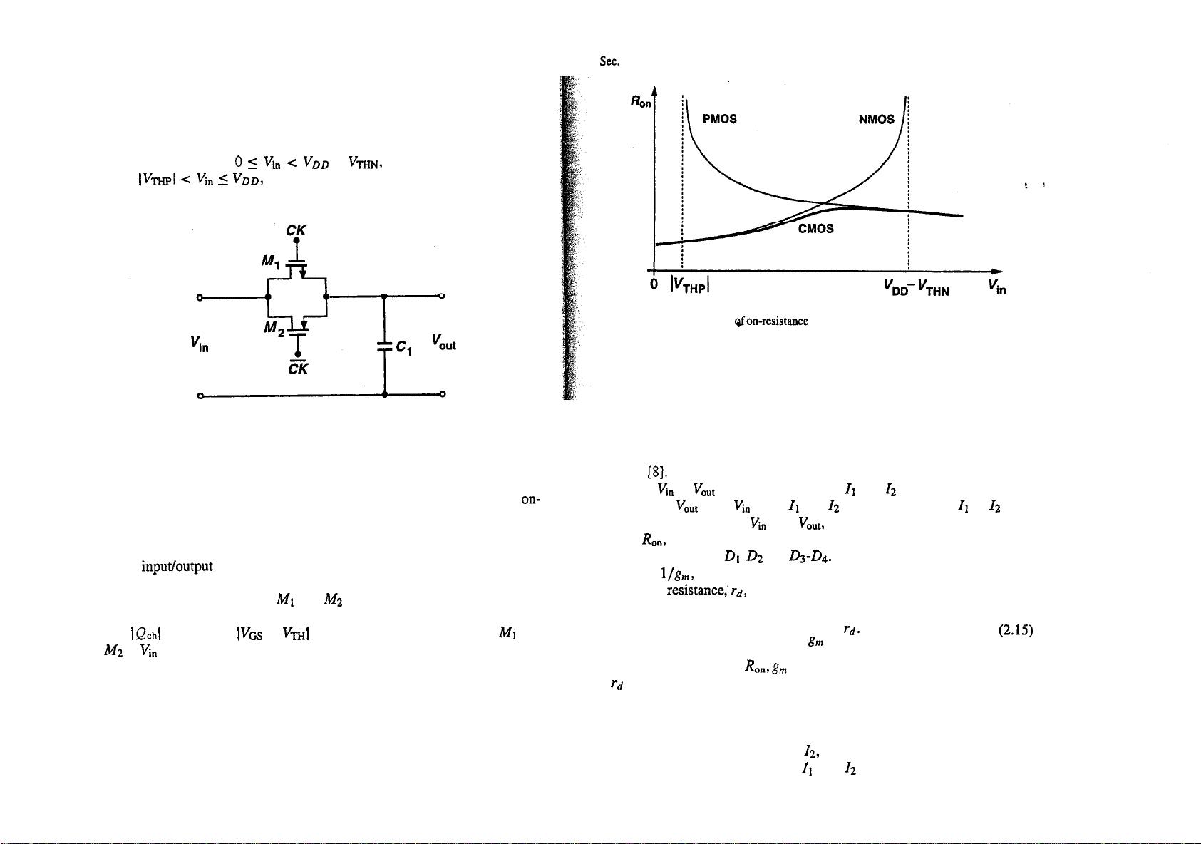
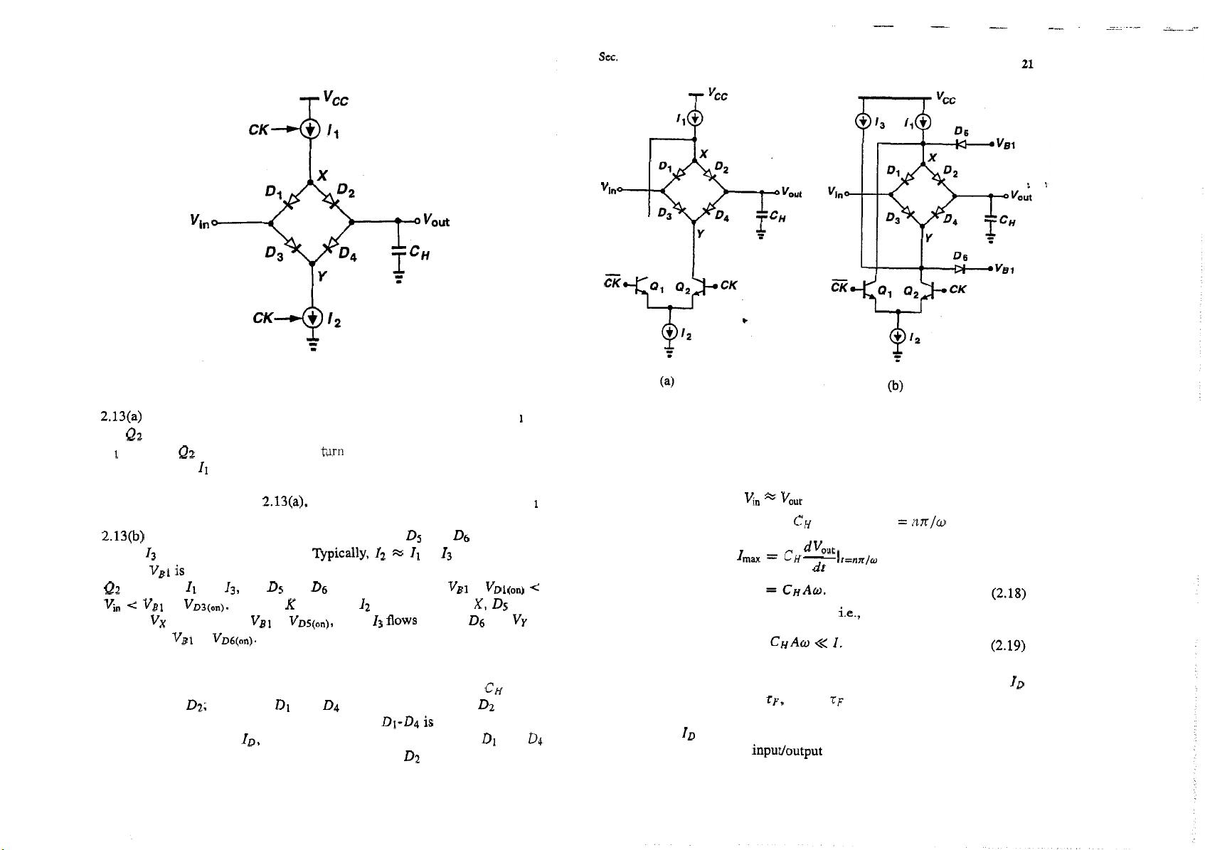
Diode switches such as that of Figure 2.13 operate with clock voltage
swings roughly an order of magnitude smaller than those of
MOS
cir
-
cuits, allowing sharper edges and better definition of sampling points
in
time. For this reason and because of lower noise
in
ECL
circuits
than in
MOS
circuits, diode switches have a potentially lower jitter
than their
MOS
counterparts.
The input voltage range of
MOS
sampling circuits is generally larger
than that of diode switches, thus allowing a wider dynamic range.
MOS
switches introduce no dc level shift (offset) from the input to
the output if the following circuit draws no current. Diode bridges,
on the other hand, suffer from a finite offset caused by mismatches in
current sources and diodes.
Diode switches are typically much more complex and dissipate much
more power than
MOS
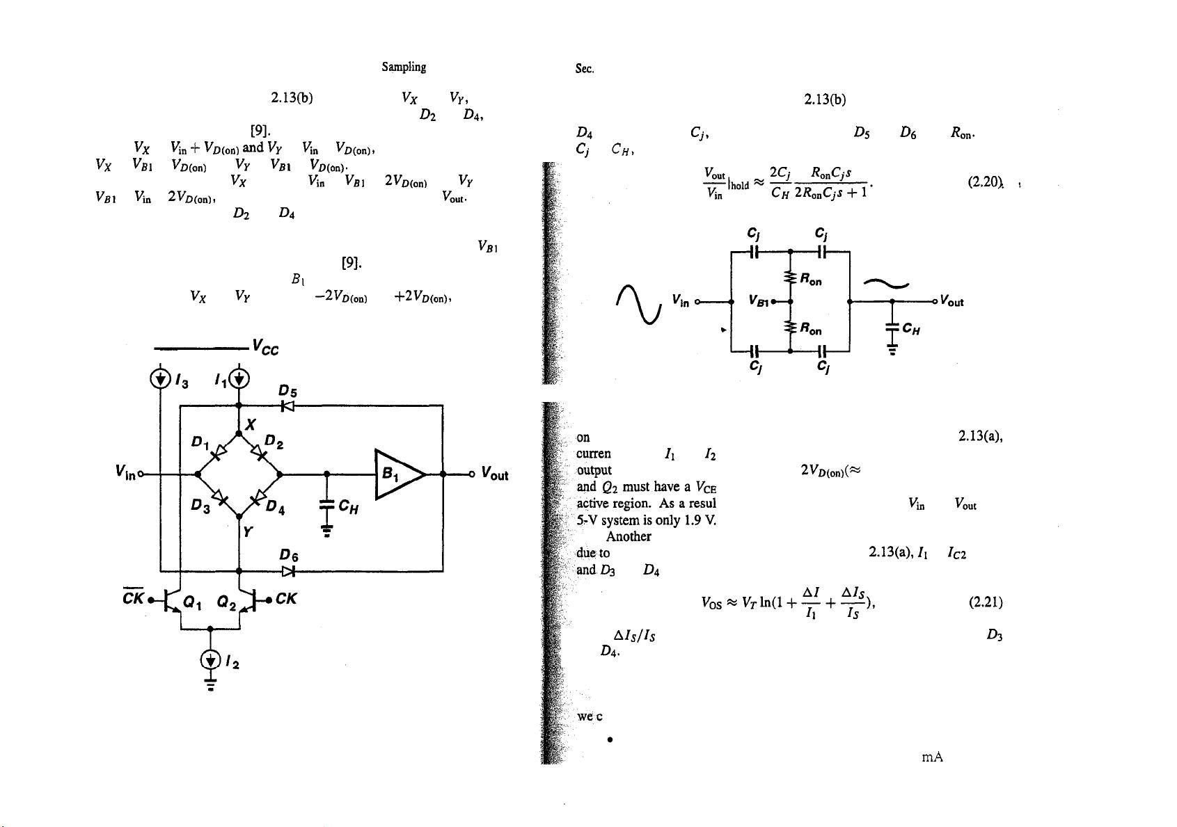
sampling circuits. The circuit of Figure
2.13(b), for example, requires at least six diodes, a differential pair,
and three current sources whose magnitudes and variations with tem
-
perature and process must be well
-
controlled.
A
MOS
sampling
switch, on the other hand, consists of one or two transistors. While
this difference in complexity and power dissipation may not be sig
-
nificant for a single SHA, it becomes important if a sampled
-
data
system such as an
A/D
converter or a filter requires a great number
of sampling switches.
2.3.4
Improvements in
MOS
Switch Performance
The simplicity of
MOS
switches has made them attractive for large
-
scale
analog integrated circuits. However, as discussed in previous sections,
MOS
devices suffer from large on
-
resistance and substantial charge stored in their
channel. In fact, the strong trade
-
off between these two parameters limits the
level of speed
-
accuracy that can be achieved in a simple circuit such as that
of Figure
2.5.
We can formulate this trade
-
off by defining a figure of merit:
F
=
[fpedestal error)
.
(acquisition time)]-'
(2.22)
Sec.
2.3
Sampling
Switches
25
The pedestal error is
Qch
AV,
=
-
~CH
where we have assumed half of the channel charge of the switch is injected
onto
CH
and neglected clock feedthrough. The acquisition time constant is
Note that since
taCq
depends on the gate
-
source voltage and hence varies with
input, modeling the acquisition behavior with a single time constant is only a
rough approximation.
From (2.24) and
(2.26), it follows that
This equation indicates that, in a given
CMOS
technology, the
MOS
sampling
circuit of Figure 2.5 does not achieve
a
speed
-
accuracy product higher than
roughly
~/.L,/L~.
This product is further degraded by clock feedthrough.
In order to relax the trade
-
off given by (2.28), a number of circuit tech
-
niques have been proposed, two of which are illustrated in Figure 2.16. In
Figure
2.16(a), a dummy device
M2
with half the width of the sampling switch
MI
(and the same length) is added and driven by
m,
the complement of the
sampling clock
CK
[lo]. In this circuit, when
MI
turns off and injects charge
onto
CH,
M2
turns on and absorbs charge from
CH
in its channel.
Thus,
if exactly half of the
MI
channel charge is injected onto
CH,
then complete
cancellation occurs and the held voltage on
CH
is not corrupted by the charge
injection. However, the fraction of channel charge injected by
MI
onto its
source and drain depends on the impedance seen at the input and output nodes
and the clock transition speed
[6], indicating that
CH
may not receive half
of the
MI
channel charge and that this scheme may not provide accurate
cancellation.
Figure
2.16(b) shows another sampling configuration, where the circuit
is implemented in differential form
[l 11.
In
this topology,
Vin,
1
and
Vin,2
are differential inputs (i.e., they vary by the same amount but in opposite
