Spartan-3 1.2V FPGA Family: Functional Description
12 www.xilinx.com DS099-2 (v1.2) July 11, 2003
1-800-255-7778 Advance Product Specification
40
R
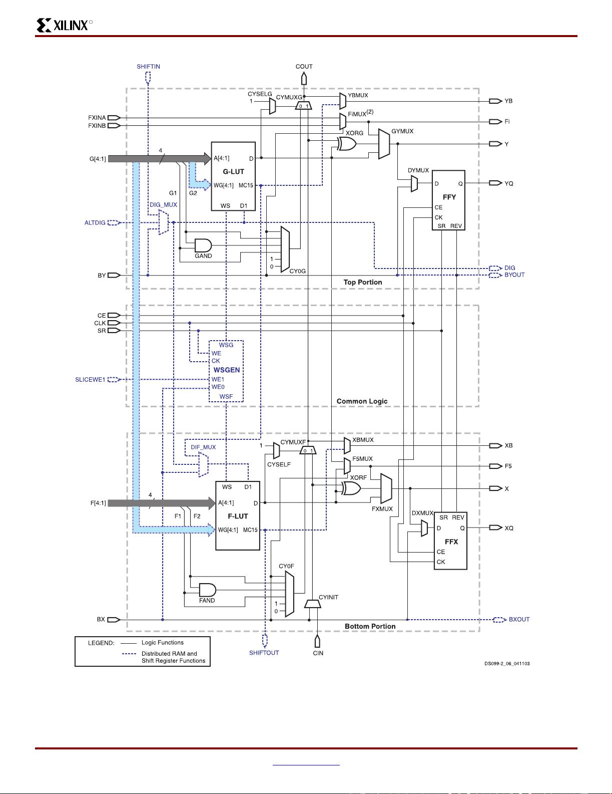
The carry chain, together with various dedicated arithmetic
logic gates, support fast and efficient implementations of
math operations. The carry chain enters the slice as CIN
and exits as COUT. Five multiplexers control the chain:
CYINIT, CY0F, and CYMUXF in the lower portion as well as
CY0G and CYMUXG in the upper portion. The dedicated
arithmetic logic includes the exclusive-OR gates XORF and
XORG (upper and lower portions of the slice, respectively)
as well as the AND gates GAND and FAND (upper and
lower portions, respectively).
Main Logic Paths
Central to the operation of each slice are two nearly identi-
cal data paths, distinguished using the terms top and bot-
tom. The description that follows uses names associated
with the bottom path. (The top path names appear in paren-
theses.) The basic path originates at an interconnect-switch
matrix outside the CLB. Four lines, F1 through F4 (or G1
through G4 on the upper path), enter the slice and connect
directly to the LUT. Once inside the slice, the lower 4-bit
path passes through a function generator "F" (or "G") that
performs logic operations. The function generator’s Data
output, "D", offers five possible paths:
1. Exit the slice via line "X" (or "Y") and return to
interconnect.
2. Inside the slice, "X" (or "Y") serves as an input to the
DXMUX (DYMUX) which feeds the data input, "D", of
the FFY (FFX) storage element. The "Q" output of the
storage element drives the line XQ (or YQ) which exits
the slice.
3. Control the CYMUXF (or CYMUXG) multiplexer on the
carry chain.
4. With the carry chain, serve as an input to the XORF (or
XORG) exclusive-OR gate that performs arithmetic
operations, producing a result on "X" (or "Y").
5. Drive the multiplexer F5MUX to implement logic
functions wider than four bits. The "D" outputs of both
the F-LUT and G-LUT serve as data inputs to this
multiplexer.
In addition to the main logic paths described above, there
are two bypass paths that enter the slice as BX and BY.
Once inside the FPGA, BX in the bottom half of the slice (or
BY in the top half) can take any of several possible
branches:
1. Bypass both the LUT and the storage element, then exit
the slice as BXOUT (or BYOUT) and return to
interconnect.
2. Bypass the LUT, then pass through a storage element
via the D input before exiting as XQ (or YQ).
3. Control the wide function multiplexer F5MUX (or
F6MUX).
4. Via multiplexers, serve as an input to the carry chain.
5. Drives the DI input of the LUT. See Distributed RAM
section.
6. BY can control the REV inputs of both the FFY and FFX
storage elements. See Storage Element Section.
7. Finally, the DIG_MUX multiplexer can switch BY onto to
the DIG line, which exits the slice.
Other slice signals shown in Figure 6, page 11 are dis-
cussed in the sections that follow.
Function Generator
Each of the two LUTs (F and G) in a slice have four logic
inputs (A1-A4) and a single output (D). This permits any
four-variable Boolean logic operation to be programmed
into them. Furthermore, wide function multiplexers can be
used to effectively combine LUTs within the same CLB or
across different CLBs, making logic functions with still more
input variables possible.
The LUTs in both the right-hand and left-hand slice-pairs
not only support the logic functions described above, but
also can function as ROM that is initialized with data at the
time of configuration.
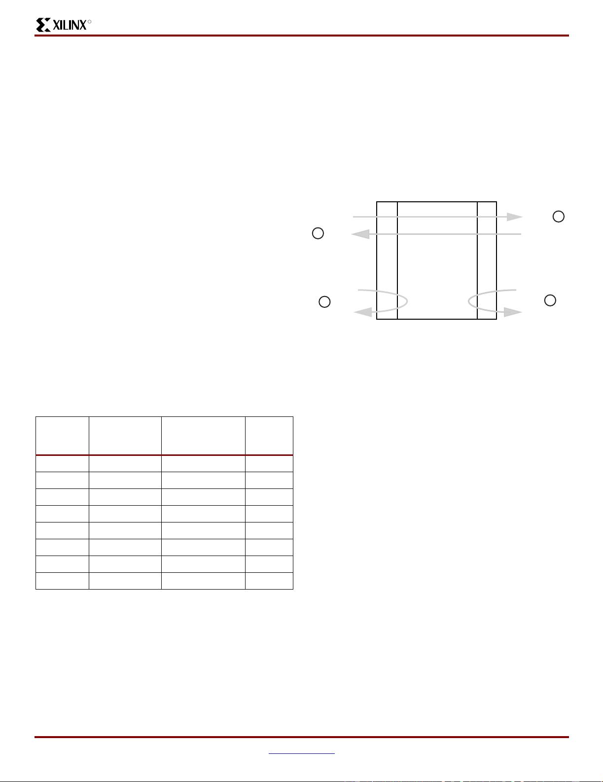
The LUTs in the left-hand slice-pair (even-numbered col-
umns such as X0 in Figure 5) of each CLB support two
additional functions that the right-hand slice-pair (odd-num-
bered columns such as X1) do not.
First, it is possible to program the “left-hand LUTs” as dis-
tributed RAM. This type of memory affords moderate
amounts of data buffering anywhere along a data path. One
left-hand LUT stores 16 bits. Multiple left-hand LUTs can be
combined in various ways to store larger amounts of data. A
dual port option combines two LUTs so that memory access
is possible from two independent data lines. A Distributed
ROM option permits pre-loading the memory with data dur-
ing FPGA configuration For more information, see the Dis-
tributed RAM section.
Second, it is possible to program each left-hand LUT as a
16-bit shift register. Used in this way, each LUT can delay
serial data anywhere from one to 16 clock cycles. The four
left-hand LUTs of a single CLB can be combined to produce
delays up to 64 clock cycles. The SHIFTIN and SHIFTOUT
lines cascade LUTs to form larger shift registers. It is also
possible to combine shift registers across more than one
CLB. The resulting programmable delays can be used to
balance the timing of data pipelines.
Block RAM Overview
All Spartan-3 devices support block RAM, which is orga-
nized as configurable, synchronous 18Kbit blocks. Block
RAM stores relatively large amounts of data more efficiently
than the distributed RAM feature described earlier. (The lat-
ter is better suited for buffering small amounts of data any-
where along signal paths.) This section describes basic
Block RAM functions. For more information, see
XAPP463:
Using Block RAM in Spartan-3 FPGAs.


