"电子产品辐射手册-TI:详解空间与地面辐射原理及应对方法"
需积分: 5 151 浏览量
更新于2024-04-11
收藏 7.79MB PDF 举报
The "Radiation Handbook for Electronics" by Texas Instruments (TI) is a comprehensive guide that delves into the principles, impacts, and mitigation methods of radiation in electronic products. This handbook is a valuable resource for engineers and designers working in space, industrial, and terrestrial applications.
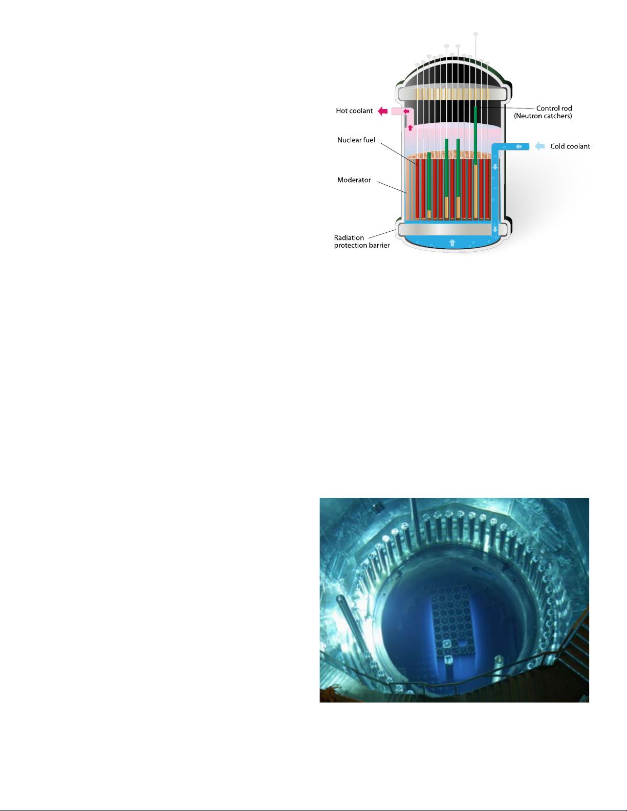
The handbook begins with a foreword from Texas Instruments that highlights their expertise and experience in space flight. Chapter 1 explores the different radiation environments, including the space radiation environment, terrestrial radiation environment, and artificial radiation environments. By understanding these environments, engineers can better protect electronic devices from the damaging effects of radiation.
Chapter 2 delves into radiation effects and mitigation strategies. By understanding how radiation impacts electronic components, designers can implement protective measures to ensure reliable performance in harsh environments. The handbook also provides practical tips and techniques for reducing radiation effects in electronic products.
One valuable resource highlighted in the handbook is a compendium of blog posts on op amp design topics by Bruce Trump. These blog posts offer practical insights and advice for designing electronic circuits that can withstand radiation exposure.
Overall, the "Radiation Handbook for Electronics" is a valuable resource for engineers and designers working in the field of electronic products. By understanding the principles of radiation, its impacts, and mitigation strategies, engineers can design robust and reliable electronic products that can withstand the rigors of space, industrial, and terrestrial applications. Texas Instruments' expertise in this field shines through in this comprehensive and informative handbook.
15
Radiation Handbook for Electronics Texas Instruments
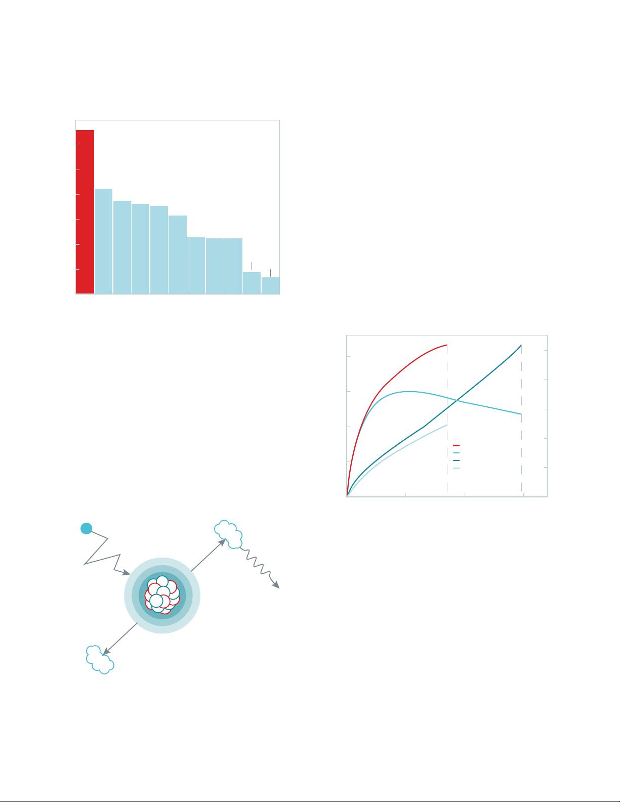
neutrons; however, its reaction cross-section is nearly 1 million
times smaller, and its reaction products (gamma rays) generally do
not cause problems. The thermal neutron capture cross-section
of
10
B is extremely high compared to most other isotopes present
in semiconductor materials (three to seven orders of magnitude
higher), as illustrated in Figure 1-18.
Unlike most isotopes that emit relatively harmless gamma photons,
after absorbing a thermal neutron, the
10
B nucleus breaks apart
with an accompanying release of energy in the form of an excited
7
Li recoil nucleus and an alpha particle. A prompt gamma photon
is also emitted from the lithium recoil soon after fission occurs. In
the
10
B(n,a)
7
Li reaction, the alpha particle and lithium nucleus are
emitted in opposite directions to conserve momentum. The lithium
nucleus is emitted with a kinetic energy of 0.840 MeV 94% of the
time and 1.014 MeV 6% of the time. The alpha particle is emitted
with an energy of 1.47 MeV, as shown in Figure 1-19.
The lithium recoil has a peak LET of 25 fC/μm, while that of the
alpha particle is 16 fC/μm. In most cases, calculations have shown
that the range of the alpha particle and lithium recoils in silicon and
silicon oxide is very limited: less than 1.5 mm. If the reaction occurs
more than 1 mm away from sensitive device nodes (deeper in the
substrate or in the layers over the silicon), neither the lithium recoil
nor alpha particle will have sufficient energy to induce SEEs.
Figure 1-20 shows the lineal charge generation and range of
both secondary products. Generally, only
10
B in close proximity to
the active silicon layer needs to be considered. For conventional
semiconductor processes, BPSG is the dominant source of boron
reactions, and in some cases can be the primary cause of soft
errors.
[41-43]
The alpha and the lithium recoils are both capable
of inducing SEEs in microelectronics, particularly in advanced
low-voltage technologies. The event rate from the
10
B(n,a)
7
Li
mechanism is a function of the thermal neutron flux, the thermal
neutron cross-section for the reaction and the amount of
10
B
in the device close to the active silicon device layers. Several
groups have measured the terrestrial thermal neutron flux and it is
between 4-20 n/cm
2
-hr, basically a little less or similar in magnitude
to the high-energy neutron flux. The
10
B(n,a)
7
Li reaction has a
thermal neutron cross-section of 3,838 barns (1 barn = 10
-24
cm
2
per nucleus).
Assuming a 1-cm
2
device area covered with a 1-mm layer of BPSG
doped with 8% boron, an upper bound for the SEE event rate can be
calculated by assuming that one of the two secondary products will
produce a detectable SEE. Because the secondaries are emitted in
opposite directions, only one of them will traverse the active devices.
Actually, since the secondary products will be emitted in or near
the active silicon device volumes, it is very likely that each event will
be capable of upsetting a sensitive volume. In any case, using the
assumptions above, an event rate of 0.0126 reactions/hr-cm
2
is
the upper bound, or, assuming that each event is an upset, a failure
rate of 17 kFIT. Clearly, this is an overestimation, but compared to
Figure 1-18. Comparison of thermal neutron capture cross-sections
for
10
B and several common semiconductor materials. This plot
demonstrates the anomalously high thermal neutron reaction
cross-section of
10
B. Note, a “barn” is a nuclear physics unit of area
equivalent to 10
-24
cm
2
.
Figure 1-20. Differential charge generation and range in silicon as a
function of particle energy from the alpha particle and lithium recoil
produced by the
10
B(n,a)
7
Li reaction.
[44]
Figure 1-19. Capture of a thermal neutron by a
10
B nucleus and the
secondary products: an alpha particle, a lithium recoil nucleus and
prompt gamma photon.
18- 3387 Rotation Graphics Chapter 2
Round 2
Figure 2.20 Figure 2.21
Thermal neutron
4
He
10
B
1.47 MeV
0.84 MeV
dQ/dx (fC/µm)
Range in silicon (µm)
Ion energy (MeV)
0
5
10
20
15
0
1
2
4
5
3
0.0 0.5 1.0 1.5
Li dQ/dx in silicon
He dQ/dx in silicon
He range in silicon
Li range in silicon
18- 3387 Rotation Graphics Chapter 2
Round 2
Figure 2.20 Figure 2.21
Thermal neutron
4
He
10
B
1.47 MeV
0.84 MeV
dQ/dx (fC/µm)
Range in silicon (µm)
Ion energy (MeV)
0
5
10
20
15
0
1
2
4
5
3
0.0 0.5 1.0 1.5
Li dQ/dx in silicon
He dQ/dx in silicon
He range in silicon
Li range in silicon
18- 3387 Rotation Graphics Chapter 2
Round 2
Figure 2.17 Figure 2.19
% Change in neutron flux
Time
-30%
-25%
-20%
-15%
-10%
-5%
0%
11/1997 3/1999 8/2000 12/2001 5/2003 9/2004
Solar eruptions follow the
“11-year sun-spot cycle”
σ
nth
(barns)
10
-3
10
-2
10
-1
10
0
10
1
10
2
10
3
10
4
Boron-10
Boron-11
Tungsten
Titanium
Arsenic
Cooper
Nitrogen
Aluminum
Silicon
Phosphorus
Oxygen
剩余117页未读,继续阅读
2022-10-26 上传
2022-07-05 上传
2022-10-28 上传
2019-09-05 上传
2022-10-25 上传
2022-10-25 上传
2022-11-27 上传
2023-02-08 上传
2023-02-08 上传

hongny1022
- 粉丝: 0
- 资源: 3
 我的内容管理
展开
我的内容管理
展开


最新资源
- C语言快速排序算法的实现与应用
- KityFormula 编辑器压缩包功能解析
- 离线搭建Kubernetes 1.17.0集群教程与资源包分享
- Java毕业设计教学平台完整教程与源码
- 综合数据集汇总:浏览记录与市场研究分析
- STM32智能家居控制系统:创新设计与无线通讯
- 深入浅出C++20标准:四大新特性解析
- Real-ESRGAN: 开源项目提升图像超分辨率技术
- 植物大战僵尸杂交版v2.0.88:新元素新挑战
- 掌握数据分析核心模型,预测未来不是梦
- Android平台蓝牙HC-06/08模块数据交互技巧
- Python源码分享:计算100至200之间的所有素数
- 免费视频修复利器:Digital Video Repair
- Chrome浏览器新版本Adblock Plus插件发布
- GifSplitter:Linux下GIF转BMP的核心工具
- Vue.js开发教程:全面学习资源指南
