14 Chapter #1
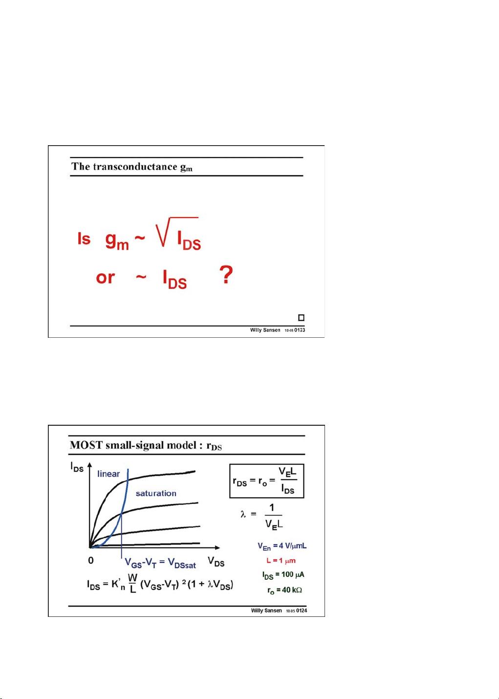
length. Therefore, we prefer to use instead another parameter V
E
. It is constant for a certain
technology. It is different for a nMOST and a pMOST. Its dimension is V/mm.
The output resistance is then easily described. An example is given.
In models used for simulators (such as SPICE) several parameters are required to describe
the output resistance. This model based on parameter V
E
, is the simplest one and is only used
for hand calculations. It only provides limited accuracy.
Parameter V
E
is the fourth technological parameter that we find: we have had up till now n,
V
T
, KP and V
E
.
Design parameters up till now are L and V
GS
−V
T
.
0125
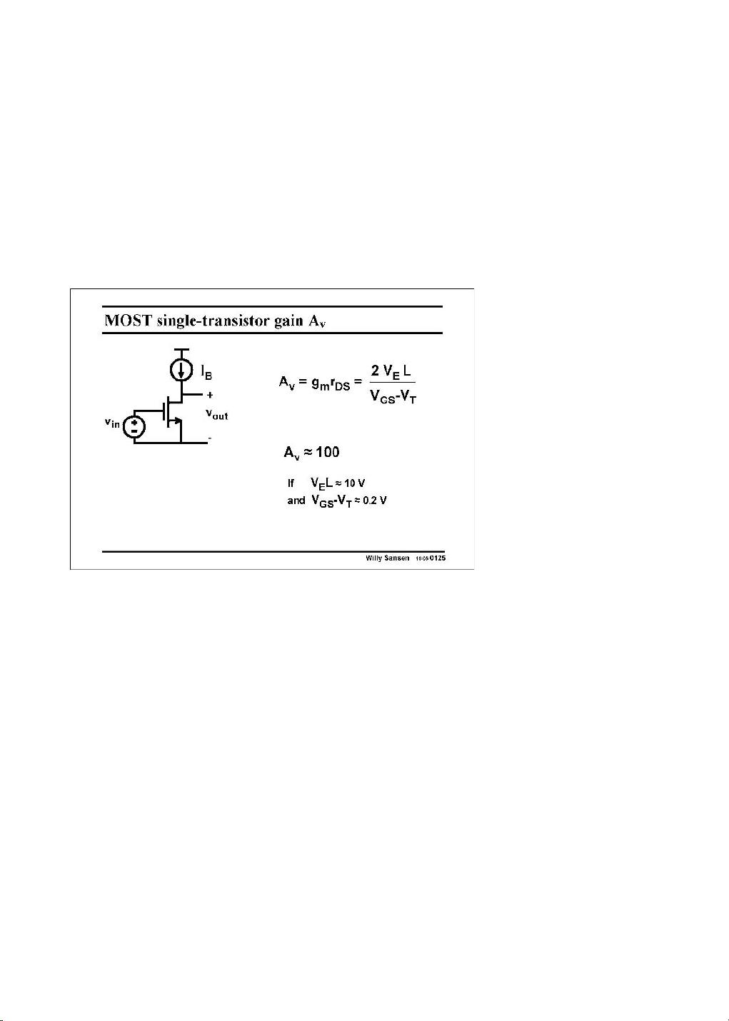
Let us now investigate how
much gain can be provided
by a single-transistor ampli-
fier, biased by a current
source with value I
B
.
The voltage gain is simply
given by g
m
r
DS
or the
expression in this slide. Note
that the current drops out
as both parameters are cur-
rent dependent.
It is clear that if we are
interested in large gain, we
will have to choose a large
channel length, normally
much larger than the mini-
mum channel length of the technology used. Also we have to choose a value of V
GS
−V
T
which
is as small as possible. A reasonable value is 0.2 V. Reasons for this choice will be given later.
In order to obtain a voltage gain of 100, relatively large channel lengths are now necessary.
If for some other reason we want to use the minimum channel length (for example for speed)
then we will have to use circuit techniques to enhance the gain. Examples are cascodes, gain
boosting, current starving, bootstrapping, etc.
Deep submicron CMOS technologies only provide very limited gain. All possible circuit
techniques will have to be used to provide large gain.
Finally, note that such an amplifier (as most amplifiers are inverting), the output voltage
increases when the input voltage decreases. This is why some authors add a minus sign to the
expression of the gain.
0126
Indeed, for each transistor in the signal path, two independent choices will have to be made in
the design procedure. They are the values of L and V
GS
−V
T
. A single-transistor amplifier can
give a large amount of gain provided its L is large and its V
GS
−V
T
is small. This will apply to
all applications where high gain, low noise and low offset are most important, such as in
operational amplifiers.
