2536 IEEE JOURNAL OF SOLID-STATE CIRCUITS, VOL. 4 7, NO. 10, OCTOBER 2012
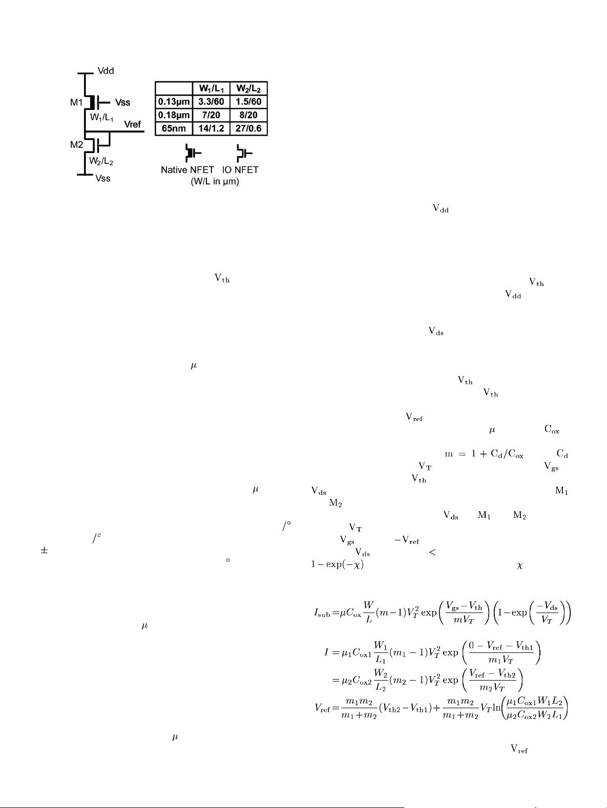
Fig. 2. Schematic of proposed 2T voltage reference.
ture points [13], [33], [34]. Due to this ultra-low power con-
sumption, the pro posed voltage reference need no duty-cycling
for saving power, elim inating start-up issues. The design uses
subthreshold-biased devices with distinct
levels, e.g., one
regular thick oxide and one native device for achieving a stable
output voltage. As a result, the number of fabrication masks is
not increased.
Since semiconducto r process variations lead to spreads in
temperature coefficient (TC) and output voltage, w e collected
statistical result s by measuring 4 9 2T voltage re fere nce proto-
types in two separate runs of 0.13
m CMOS. These exten-
sive measurement results provide a better understanding of the
advantages and limitations of the proposed design. Measure-
ment results indicate that the 2T voltage reference exhibits mod-
erate spread in TC and output voltage due t o die-to-die and
run-to-run process variations. Such process sensitivity is typi-
cally addressed through trimming. Ho wever, trimming can be
a time and cost intensive process [6]. We propose a d igitally
trimmable version of the 2T voltage reference to i mp rove TC
and output voltage accuracy across dies while enabling reason-
able trim time and cost [32]. Measurements in 0.13
mCMOS
show that the proposed trimm ing enables tight distributions of
TC and nominal output voltage across 25 dies. After one-tem -
perature point digital trimmin g, TCs lie between 13.5 ppm
C
and47ppm
C w h ile the nominal output voltage v aries by
0.35% from the m ean value. The typical trimmable voltage
reference consumes 29.5 pW at 0.5 V and 25
C.
We also propose several variants of the 2T voltage reference,
including circuits to generate a specific output voltage, either
higher or lower than its nominal value. We also demonstrate
the 2T voltage referen ce with specific tem perature dependence,
PTAT o r C TAT, i n 0 .13
m CMOS. Technology portability is
also investigated. Due the wide range of supply voltage scala-
bility a nd simple top olo gy, the proposed designs often involve
only resizing o f two transistors, facilitating i ts use as an intel-
lectual property (IP) block across different technologies.
The remainder of this paper is organized as follows. Section II
introduces the design of the proposed 2T voltage reference
along with the governing eq uations for T C a n d line sensitivity
(LS). Section III describes basic measurement r esults of the
2T voltage reference in 0.13
m CMOS and compares to
previous work. Section IV investigates the impact of process
variations on the performance of the proposed 2T voltage
reference w it h additional silicon measurement results. We also
propose a assisted one temperature point trimming method,
and show that it tightens the performance spread in silicon
measurements. Section V introduces several variants of t he
2T voltage references including measured results. Section V I
demonstrates the easy port a bil ity of the 2T voltage references
by providing measurement results in tw o additional C M O S
technology nodes, while Section VII concludes the paper.
II. 2T V
OLTAGE REFERENCE DESIGN AND ANALYS IS
As mentio ned above, the use of amplifiers and/or saturated
MOSFETs is a key barrier to the scalability of power consump-
tion and minimum functional
in voltage references. There-
fore, we seek to eliminate them while m a int a ini n g output in-
sensitivity to temperature and supply voltage. To this end, we
propose the 2T vo ltage reference shown in Fig. 2. Two different
device types are used; in this case a native device for M1 and a
thick oxide inpu t/o utp ut (I/O) device for M2. The native device
is identical to a standard M OSFET but has a near-zero
.Both
devices have thick gate oxides to support a high
. Native de-
vices are widely available in modern foundry technologies [2 4],
[25] and do not incur additional m ask step s. One common use
of n a tiv e devices is t o limit
in thin o xide dev ices by con-
necting them in series, as shown in [26]. They have also been
used in b andg ap voltage reference circuits [8] and image sensors
[27]. Although we us e a native device for M1, any com bination
of two d evices with a considerable
difference can be used
for the 2T voltage reference. The required
difference is dis-
cussed later.
The outpu t voltage
can be modeled by (1), the well-
known subthreshold current equation where
is mobility, is
oxide capacitance, W is transistor width, L is transistor length,
m is subthreshold slope factor (
where
is depletion capacitance), is therm al voltage (kT/q), is
gate and source voltage,
is transistor threshold voltage, and
is drain to source voltag e. Setting the cu rrent through
and equal leads to (2), which holds given that 1) both de-
vices are in weak inversion, 2)
for and is greater
than 5–6
, and 3) M1 follows the subthreshold current equa-
tion at
down to . The second condition relates to the
minimum
that ensures 1% loss of accuracy given that
equals 0.982, 0.99 3, and 0.997 when is 4, 5, and
6, respectively. The third condition ensures that gate induced
drain leakage (GIDL) is not signi fican t at the operating point.
(1)
(2)
(3)
From (2), we obtain an analytical solution for
as shown
in (3), where both the first and second terms are either pro-
portional or complemen tary to absolute temperature. Note that


