3.1.2 Loss of Input Clock - Limp Mode
3.1.3 XCLKOUT
Handling of Different Hardware Building Blocks
www.ti.com
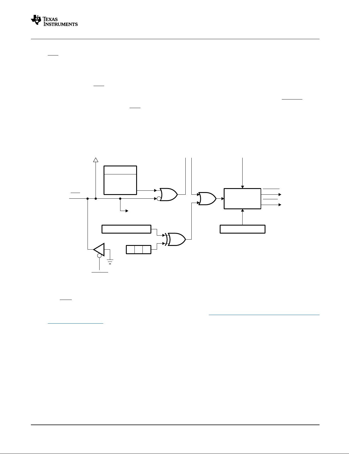
Connect the output of the external oscillator to the F280x and F28xxx parts as shown in Figure 4, based
upon the level. It is important to connect X1 or XCLKIN to ground as shown. If they are left open, the
frequency of CLKOUT will be incorrect and the DSC may not work properly.
Figure 4. Connecting External Oscillator to F280x/F28xxx
The F281x devices select the external clock oscillator part that toggles between 0 - V
DD
(0 – 1.8 V/1.9V).
Note: If you are using a 3.3 V external oscillator for an F281x system, use a 3.3 V to 1.8 V/1.9 V
voltage translator device equivalent to TI’s SN74LVC1G14 - SN74LVC1G14 Single
Schmitt-Trigger Inverter Data Sheet (SCES218) .
The PLL still issues a limp-mode clock if the input clock, OSCCLK, is removed or absent. The limp-mode
clock continues to clock the CPU and peripherals at a typical frequency of 1 MHz - 5 MHz. Limp mode is
not specified to work from power-up, but only after input clocks have been present. In PLL bypass mode,
the limp mode clock from the PLL is automatically routed to the CPU if the input clock is removed or
absent. The watchdog counter stops decrementing with the failure of the input clock and does not change
with the limp-mode clock. These conditions could be used by the application firmware to detect the input
clock failure and initiate a necessary shut-down procedure for the system.
Note: Applications in which the correct CPU operating frequency is absolutely critical should
implement a mechanism by which the DSC is held in reset should the input clocks ever fail.
For example, an R-C circuit can be used to trigger the XRS pin of the DSC, should the
capacitor ever get fully charged. An I/O pin can be used to discharge the capacitor on a
periodic basis to prevent it from getting fully charged. Such a circuit would also help in
detecting failure of the Flash memory and the V
DD3VFL
rail.
The output clock signal, derived from SYSCLKOUT, is available on XCLKOUT as a general-purpose clock
source, which can be used for external wait-state generation. It also serves as a Test Point to check the
CPU clock frequency and to ensure that the PLL is working properly. At reset, XCLKOUT =
SYSCLKOUT/4; but it can be set the same as or 1/2 of SYSCLKOUT.
The XCLKOUT signal is active when reset is active. Since XCLKOUT should reflect SYSCLKOUT/4 when
reset is low, you can monitor this signal to detect if the device is being properly clocked during debug.
There is no internal pullup or pulldown on the XCLKOUT pin. The drive strength of this pin is 8 mA. If
XCLKOUT is not being used, it can be turned off by setting the CLKOFF bit to 1 in the XINTF
Configuration Register (XINTCNF2). This is an output pin of the CMOS device and should not be
terminated to ground even if it is not used.
6 Hardware Design Guidelines for TMS320F28xx and TMS320F28xxx DSCs SPRAAS1A– August 2008
Submit Documentation Feedback
4. F280x/F28xxx


