3
FN3093.3
Absolute Maximum Ratings Thermal Information
Supply Voltage V+ . . . . . . . . . . . . . . . . . . . . . . . . . . . . . . . . . . . .+6V
V- . . . . . . . . . . . . . . . . . . . . . . . . . . . . . . . . . . . -9V
Analog Input Voltage (Either Input) (Note 1) . . . . . . . . . . . . V+ to V-
Reference Input Voltage (Either Input) . . . . . . . . . . . . . . . . V+ to V-
Clock Input Voltage . . . . . . . . . . . . . . . . . . . . . . . . . . . . . GND to V+
Operating Conditions
Temperature Range. . . . . . . . . . . . . . . . . . . . . . . . . . . . 0
o
C to 70
o
C
Thermal Resistance (Typical, Note 2) . . . . . . . . . . . . .
θ
JA
(
o
C/W)
PDIP Package . . . . . . . . . . . . . . . . . . . . . . . . . . . . . 55
Maximum Junction Temperature . . . . . . . . . . . . . . . . . . . . . . .150
o
C
Maximum Storage Temperature Range . . . . . . . . . -65
o
C to 150
o
C
Maximum Lead Temperature (Soldering 10s) . . . . . . . . . . . . .300
o
C
NOTE: Pb-free PDIPs can be used for through hole wave solder
processing only. They are not intended for use in Reflow solder
processing applications.
CAUTION: Stresses above those listed in “Absolute Maximum Ratings” may cause permanent damage to the device. This is a stress only rating and operation of the
device at these or any other conditions above those indicated in the operational sections of this specification is not implied.
NOTES:
1. Input voltages may exceed the supply voltages provided the input current is limited to +100μA.
2. θ
JA
is measured with the component mounted on a low effective thermal conductivity test board in free air. See Tech Brief TB379 for details.
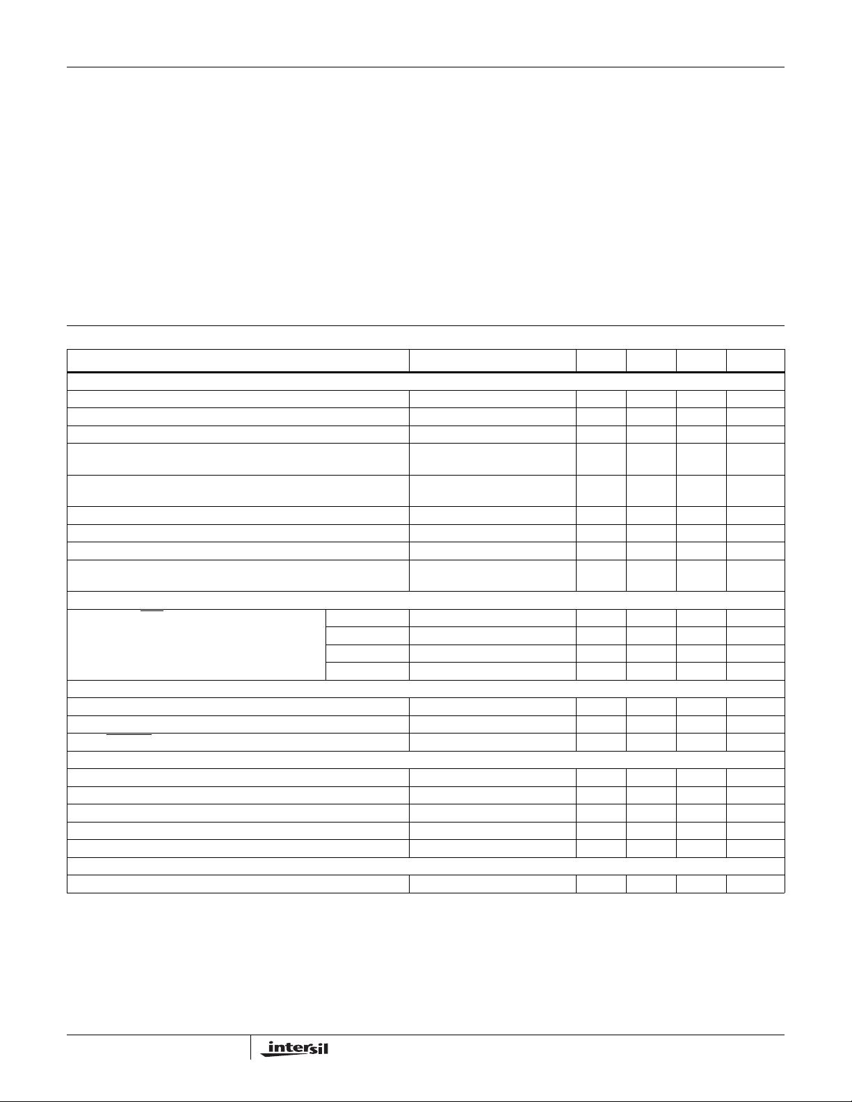
Electrical Specifications V+ = +5V, V- = -5V, T
A
= 25
o
C, f
CLK
Set for 3 Readings/s, Unless Otherwise Specified
PARAMETER TEST CONDITIONS
MIN TYP MAX UNITS
ANALOG (Notes 3, 4)
Zero Input Reading V
lN
= 0V, V
REF
= 1.000V -00000 +00000 +00000 Counts
Ratiometric Error (Note 4) V
lN
= V
REF
= 1.000V -3 0 +3 Counts
Linearity Over ± Full Scale (Error of Reading from Best Straight Line) -2V ≤ V
IN
≤ +2V - 0.5 1 LSB
Differential Linearity (Difference Between Worse Case Step of
Adjacent Counts and Ideal Step)
-2V ≤ V
IN
≤ +2V - 0.01 - LSB
Rollover Error (Difference in Reading for Equal Positive and
Negative Voltage Near Full Scale)
-V
lN
≡ +V
lN
≈ 2V - 0.5 1 LSB
Noise (Peak-to-Peak Value Not Exceeded 95% of Time), e
N
V
lN
= 0V, Full scale = 2.000V - 15 - μV
Input Leakage Current, I
ILK
V
lN
= 0V - 1 10 pA
Zero Reading Drift (Note 7) V
lN
= 0V, 0
o
C to 70
o
C-0.52μV/
o
C
Scale Factor Temperature Coefficient, T
C
(Notes 5 and 7) V
lN
= +2V, 0
o
C to 70
o
C
Ext. Ref. 0ppm/
o
C
- 2 5 ppm/×
o
C
DIGITAL INPUTS
Clock In, Run/Hold
(See Figure 2) V
INH
2.8 2.2 - V
V
INL
-1.60.8 V
I
INL
V
IN
= 0V - 0.02 0.1 mA
I
INH
V
IN
= +5V - 0.1 10 μA
DIGITAL OUTPUTS
All Outputs, V
OL
I
OL
= 1.6mA - 0.25 0.40 V
B1, B2, B4, B8, D1, D2, D3, D4, D5, V
OH
I
OH
= -1mA 2.4 4.2 - V
BUSY, STROBE
, OVERRANGE, UNDERRANGE, POLARITY, V
OH
I
OH
= -10μA 4.9 4.99 - V
SUPPLY
+5V Supply Range, V+ +4 +5 +6 V
-5V Supply Range, V- -3 -5 -8 V
+5V Supply Current, I+ f
C
= 0 - 1.1 3.0 mA
-5V Supply Current, I- f
C
= 0 - 0.8 3.0 mA
Power Dissipation Capacitance, C
PD
vs Clock Frequency - 40 - pF
CLOCK
Clock Frequency (Note 6) DC 2000 1200 kHz
NOTES:
3. Tested in 4
1
/
2
digit (20.000 count) circuit shown in Figure 3. (Clock frequency 120kHz.)
4. Tested with a low dielectric absorption integrating capacitor, the 27Ω INT OUT resistor shorted, and R
lNT
= 0. See Component Value Selection Discussion.
5. The temperature range can be extended to 70
o
C and beyond as long as the auto-zero and reference capacitors are increased to absorb the higher leakage
of the ICL7135.
6. This specification relates to the clock frequency range over which the lCL7135 will correctly perform its various functions See “Max Clock Frequency”
section for limitations on the clock frequency range in a system.
7. Parameter guaranteed by design or characterization. Not production tested.
ICL7135


