8.3.3.5 External Clock Input for PWM Generator (CLK)
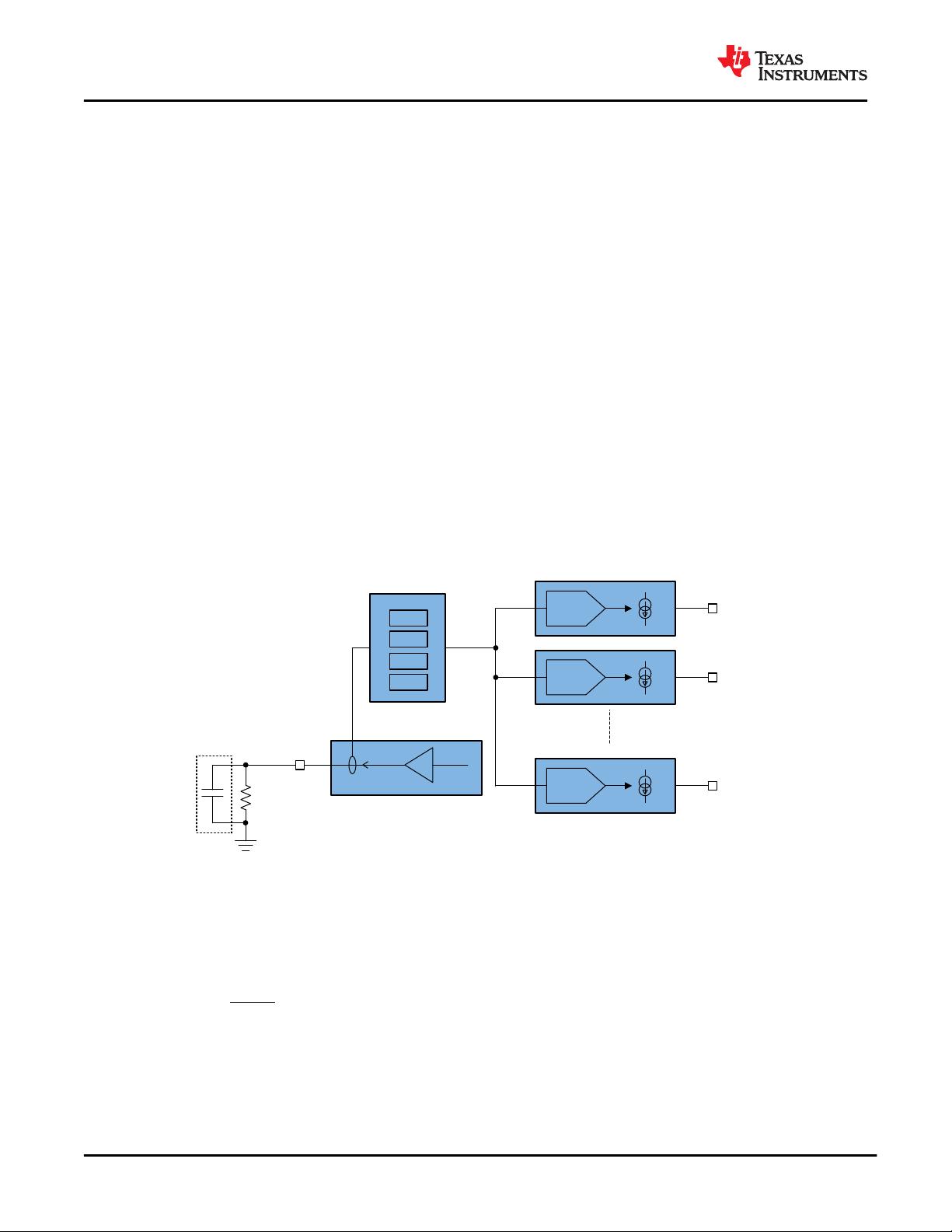
The TPS929121-Q1 has internal precision oscillator for PWM generators. In addition, the device also supports
an external clock for the PWM generator source with ADDR2/CLK input considering the synchronization
requirement.
Then external clock inputs through ADDR2/CLK pin is a multi-function pin not only for external clock input but
also for device slave address selection. The device slave address stored in EEPROM must be enabled by
burning EEP_INTADDR to 1 to release ADDR2/CLK pin for external clock input. In addition, register
CONF_EXTCLK can be used to choose the PWM generator between external input or an internal oscillator.
Writing CONF_EXTCLK to 1 enables the external clock source. The external clock frequency must be 256 times
of desired PWM dimming frequency. The external clock source is only used in PWM generation. TI recommends
that the external clock frequency be less than 1 MHz. The internal clock is recommended when high dimming
frequency is required.
8.3.3.6 External PWM Input ( PWM0 and PWM1)
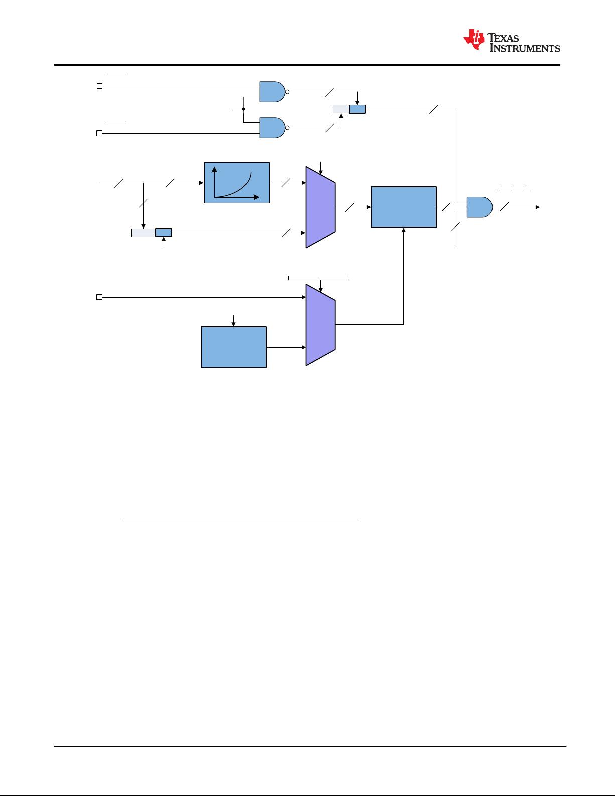
The TPS929121-Q1 has two PWM inputs that can be used to directly control OUT0-11. The both ADDR1/
PWM1 and ADDR0/ PWM0 pins are multi-function pins for not only external PWM input signal but also device
slave address selection pins. The register EEP_INTADDR must be written to 1 to release both twos for external
PWM input. When the EEP_INTADDR is 1, the ADDR0/ PWM0 is functional as external active low PWM control
input for OUT0-5 and the ADDR1/ PWM1 is functional as external active low PWM control input for OUT6-11, as
shown in Figure 8-2. Setting the register CONF_PWMOUTx to 0xFF and the register CONF_PWMLOWOUTx to
0xF is recommended when external PWM input is used. In case external PWM is not used, ADDR0/ PWM0 and
ADDR1/ PWM1 must be tied to GND when EEP_INTADDR is set to 1.
8.3.4 On-chip 8-bit Analog-to-Digital Converter (ADC)
The TPS929121-Q1 has integrated a successive-approximation-register (SAR) ADC for diagnostics. It routinely
monitors supply voltage if the ADC is idle and stores SUPPLY conversion results into ADC_SUPPLY.
To manually read the voltage of an ADC channel as listed in Table 8-2, user must write the 5-bit register
CONF_ADCCH to select channel. Once CONF_ADCCH register is written, the one time ADC conversion starts
and clears FLAG_ADCDONE register. As long as the ADC conversion is completed, the ADC result is available
in 8-bit register ADC_OUT and sets FLAG_ADCDONE to 1. Reading the ADC_OUT register also clears
FLAG_ADCDONE, and the FLAG_ADCDONE is set to 0 after reading completion.
Because the TPS929121-Q1 supports PWM control for adjusting LED brightness, the voltage on OUT0 to
OUT11 is like a pulse waveform. When the current output is enabled by setting CONF_ENCHx to 1, the ADC
measures the voltage on assigned OUTx after the channel is turned on with t
(diag_pulse)
delay time, which is
programmable by 4-bit register CONF_ODPW. When the channel is disabled by setting CONF_ENCHx to 0, the
ADC samples the voltage on assigned OUTx at off state.
The analog value can be calculated based on the read back binary code with Equation 5 and Table 8-2.
AnalogValue a k ADC_ OUT u
(5)
where
• ADC_OUT is decimal number from 0 to 255.
TPS929121-Q1
SLVSFZ4A – DECEMBER 2020 – REVISED FEBRUARY 2021
www.ti.com
20 Submit Document Feedback
Copyright © 2021 Texas Instruments Incorporated
Product Folder Links: TPS929121-Q1


