Document Number: 001-52136 Rev. *R Page 9 of 52
UART Interface
The UART interface of FX3 supports full-duplex communication.
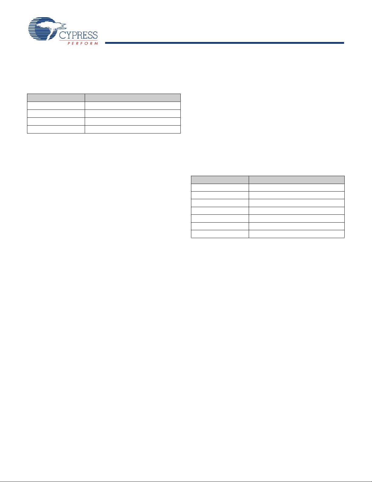
It includes the signals noted in Ta ble 1 .
The UART is capable of generating a range of baud rates, from
300 bps to 4608 Kbps, selectable by the firmware. If flow control
is enabled, then FX3's UART only transmits data when the CTS
input is asserted. In addition to this, FX3’s UART asserts the RTS
output signal, when it is ready to receive data.
I
2
C Interface
FX3’s I
2
C interface is compatible with the I
2
C Bus Specification
Revision 3. This I
2
C interface is capable of operating only as I
2
C
master; therefore, it may be used to communicate with other I
2
C
slave devices. For example, FX3 may boot from an EEPROM
connected to the I
2
C interface, as a selectable boot option.
FX3’s I
2
C Master Controller also supports multi-master mode
functionality.
The power supply for the I
2
C interface is VIO5, which is a
separate power domain from the other serial peripherals. This
gives the I
2
C interface the flexibility to operate at a different
voltage than the other serial interfaces.
The I
2
C controller supports bus frequencies of 100 kHz,
400 kHz, and 1 MHz. When VIO5 is 1.2 V, the maximum
operating frequency supported is 100 kHz. When VIO5 is 1.8 V,
2.5 V, or 3.3 V, the operating frequencies supported are 400 kHz
and 1 MHz. The I
2
C controller supports clock-stretching to
enable slower devices to exercise flow control.
The I
2
C interface’s SCL and SDA signals require external pull-up
resistors. The pull-up resistors must be connected to VIO5.
I
2
S Interface
FX3 has an I
2
S port to support external audio codec devices.
FX3 functions as I
2
S Master as transmitter only. The I
2
S interface
consists of four signals: clock line (I2S_CLK), serial data line
(I2S_SD), word select line (I2S_WS), and master system clock
(I2S_MCLK). FX3 can generate the system clock as an output
on I2S_MCLK or accept an external system clock input on
I2S_MCLK.
The sampling frequencies supported by the I
2
S interface are
32 kHz, 44.1 kHz, and 48 kHz.
Boot Options
FX3 can load boot images from various sources, selected by the
configuration of the PMODE pins. Following are the FX3 boot
options:
■ Boot from USB
■ Boot from I
2
C
■ Boot from SPI (SPI devices supported are M25P32 (32 Mbit),
M25P16 (16 Mbit), M25P80 (8 Mbit), and M25P40 (4 Mbit)) or
their equivalents
■ Boot from GPIF II ASync ADMux mode
■ Boot from GPIF II Sync ADMux mode
■ Boot from GPIF II ASync SRAM mode
Reset
Hard Reset
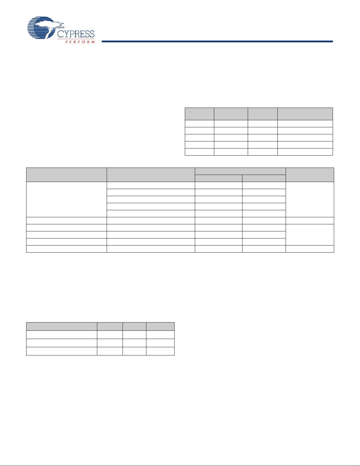
A hard reset is initiated by asserting the Reset# pin on FX3. The
specific reset sequence and timing requirements are detailed in
Figure 30 on page 42 and Table 19 on page 42. All I/Os are
tristated during a hard reset. Note however, that the on-chip
bootloader has control after a hard reset and it will configure I/O
signals depending on the selected boot mode; see AN76405 -
EZ-USB® FX3™ Boot Options for more details.
Soft Reset
In a soft reset, the processor sets the appropriate bits in the
PP_INIT control register. There are two types of Soft Reset:
■ CPU Reset – The CPU Program Counter is reset. Firmware
does not need to be reloaded following a CPU Reset.
■ Whole Device Reset – This reset is identical to Hard Reset.
■ The firmware must be reloaded following a Whole Device
Reset.
Table 1. UART Interface Signals
Signal Description
TX Output signal
RX Input signal
CTS Flow control
RTS Flow control
Table 2. FX3 Booting Options
PMODE[2:0]
[1]
Boot From
F00 Sync ADMux (16-bit)
F01 Async ADMux (16-bit)
F11 USB boot
F0F Async SRAM (16-bit)
F1F I
2
C, On Failure, USB Boot is Enabled
1FF I
2
C only
0F1 SPI, On Failure, USB Boot is Enabled
Note
1. F indicates Floating.


