RF430FRL152H, RF430FRL153H, RF430FRL154H
ZHCSD28C –NOVEMBER 2012–REVISED DECEMBER 2014
www.ti.com.cn
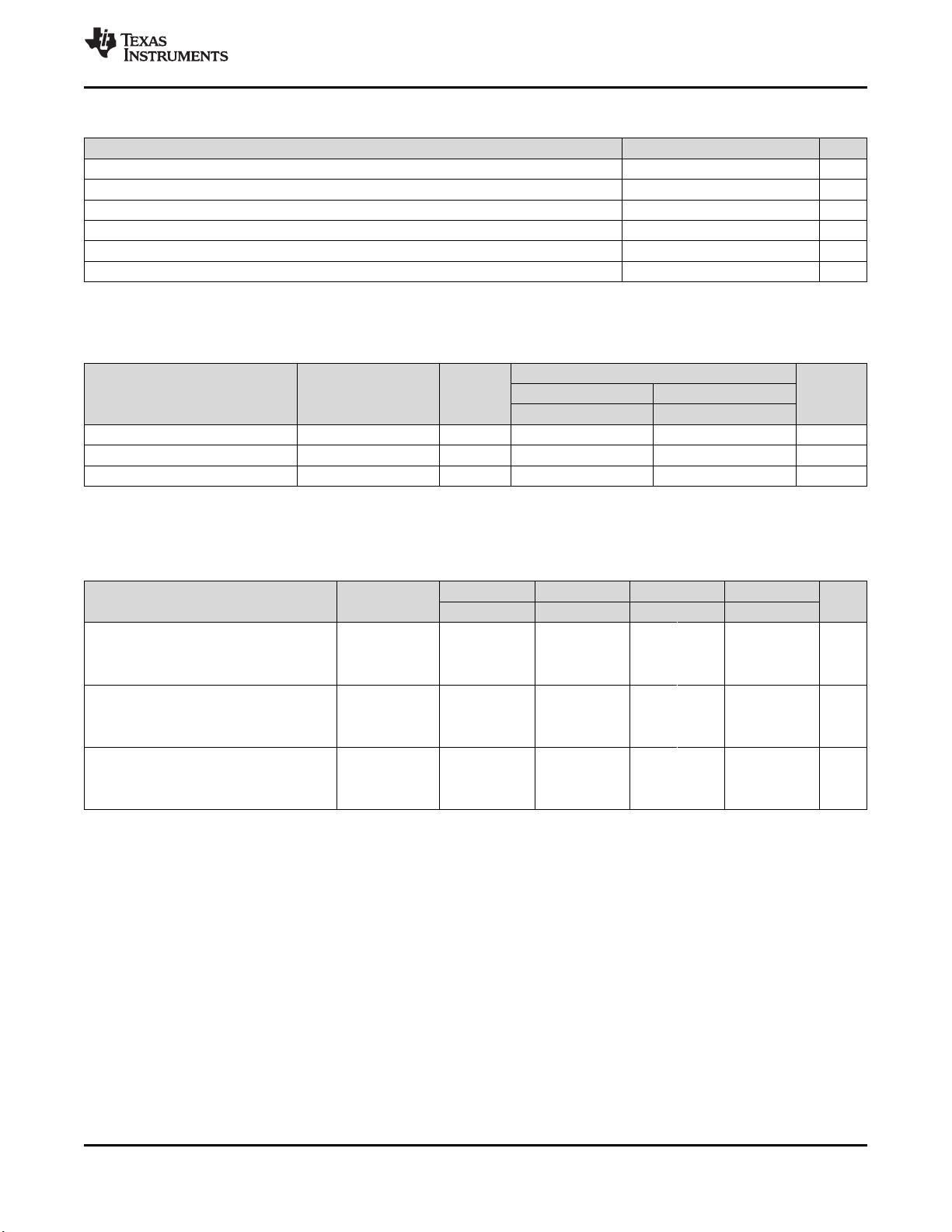
5 Specifications
5.1 Absolute Maximum Ratings
(1)
over recommended ranges of supply voltage and operating free-air temperature (unless otherwise noted)
MIN MAX UNIT
Voltage applied at V
DDB
referenced to V
SS
(V
AMR
) -0.3 1.65 V
Voltage applied at V
ANT
referenced to V
SS
(V
AMR
) -0.3 3.6 V
Voltage applied to any pin (references to V
SS
) -0.3 V
DDB
+ 0.3 V
Diode current at any device pin
(2)
±2 mA
Current derating factor when I/O ports are switched in parallel electrically and logically
(3)
0.9
Storage temperature range, T
stg
(4) (5) (6)
-40 125 °C
(1) Stresses beyond those listed under Absolute Maximum Ratings may cause permanent damage to the device. These are stress ratings
only, and functional operation of the device at these or any other conditions beyond those indicated under Recommended Operating
Conditions is not implied. Exposure to absolute-maximum-rated conditions for extended periods may affect device reliability.
(2) All voltages are referenced to V
SS
.
(3) The diode current increases to ±4.5 mA when two pins are connected, it increases to ±6.75 mA when three pins are connected, and so
on.
(4) Soldering during board manufacturing must follow the current JEDEC J-STD-020 specification with peak reflow temperatures not higher
than classified on the device label on the shipping boxes or reels. If hand soldering is required for application prototyping, peak
temperature must not exceed 250°C for a total of 5 minutes for any single device.
(5) Data retention on FRAM memory cannot be ensured when exceeding the specified maximum storage temperature, T
stg
.
(6) Programming of devices with user application code should only be performed after reflow or hand soldering. Factory programmed
information, such as calibration values, are designed to withstand the temperatures reached in the current JEDEC J-STD-020
specification.
5.2 ESD Ratings
VALUE UNIT
Electrostatic discharge (ESD)
V
ESD
Human body model (HBM), per ANSI/ESDA/JEDEC JS001
(1)(2)
±2000 V
performance
(1) JEDEC document JEP155 states that 500-V HBM allows safe manufacturing with a standard ESD control process.
(2) Low leakage pin: ADC0 has reduced ESD tolerance of ±500 V HBM.
5.3 Recommended Operating Conditions
Typical data are based on V
DDB
= 1.5 V, T
A
= 25°C (unless otherwise noted)
MIN NOM MAX UNIT
V
DDB
Supply voltage during program execution 1.45 1.65 V
V
SS
Supply voltage (GND reference) 0 V
T
A
Operating free-air temperature 0 70 °C
C
VDDB
Capacitor on V
DDB
(1)
100 nF
C
VDDSW
Capacitor on V
DDSW
(1)
2.2 µF
Charge pump capacitor between CP1 and CP2.
C
FLY
10 nF
Recommended ratio between C
FLY
and C
VDD2X
is ≥ 1:10.
(1)
Capacitor on V
DD2x
.
C
VDD2X
100 nF
Recommended ratio between C
FLY
and C
VDD2X
is ≥ 1:10.
(1)
C
VDDD
Capacitor on V
DDD
(1)
1 µF
C
SVSS
Capacitor between SVSS and V
SS
(1)
1 µF
f
SYSTEM
System frequency
(2) (3)
2 MHz
f
CLKIN
External clock input frequency 32 kHz
(1) Low equivalent series resistance (ESR) capacitor
(2) The MSP430 CPU is clocked directly with MCLK. Both the high and low phase of MCLK must not exceed the pulse duration of the
specified maximum frequency.
(3) Modules may have a different maximum input clock specification. See the specification of the respective module in this data sheet.
10 Specifications Copyright © 2012–2014, Texas Instruments Incorporated
Submit Documentation Feedback
Product Folder Links: RF430FRL152H RF430FRL153H RF430FRL154H


