"深度解析芯片封装工艺流程与图解"
需积分: 10 126 浏览量
更新于2024-04-13
3
收藏 5.06MB PPT 举报
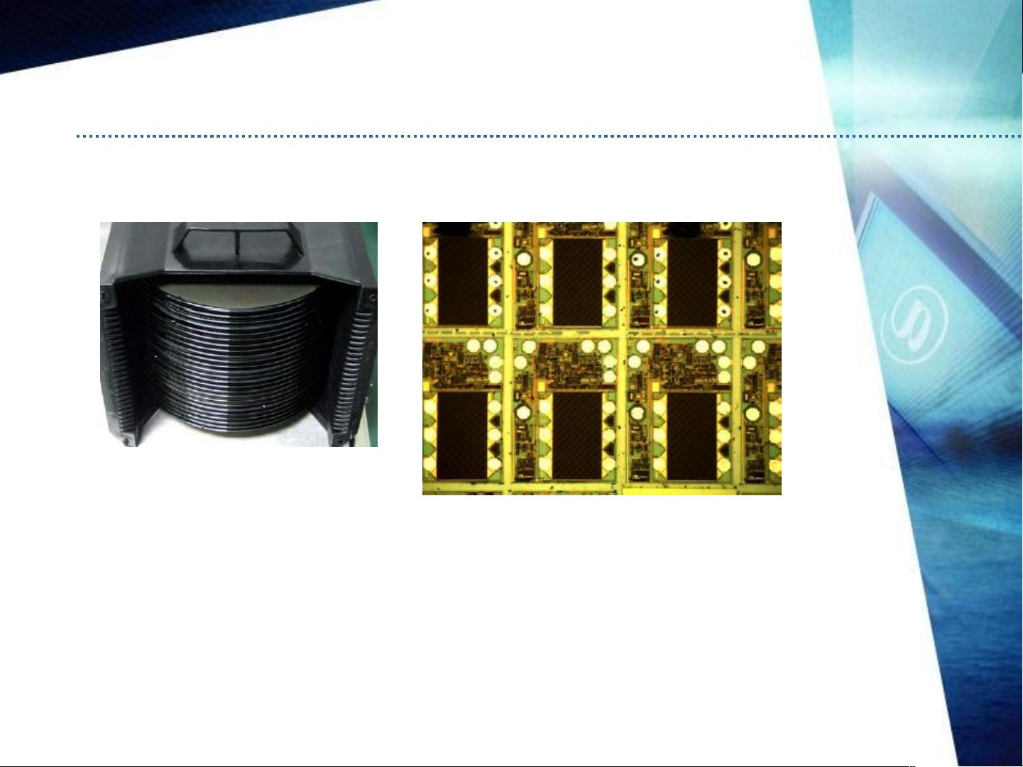
The process of IC assembly involves several key steps to prepare and package integrated circuits for use in various electronic devices. The process begins with the design of the IC, which is then manufactured on a silicon wafer in a cleanroom environment. The wafer is probed to test the functionality of the individual chips before proceeding to the assembly stage.
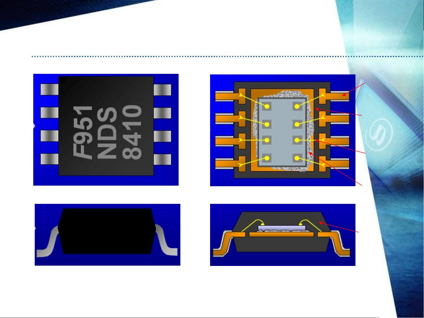
In the assembly stage, the individual chips are cut from the wafer and undergo a series of packaging steps to protect them and provide the necessary electrical connections. This packaging process involves several key components, including the substrate, wire bonding, encapsulation, and testing.
The substrate, typically made of materials such as ceramic or organic substrates, serves as a platform for the chip to be mounted on and provides the necessary electrical connections. Wire bonding is then used to connect the chip to the substrate using ultrasonic or thermosonic bonding techniques. Encapsulation follows, where the chip and wire bonds are encapsulated in a protective material such as epoxy or plastic to prevent damage from moisture and other environmental factors.
Finally, the assembled IC undergoes rigorous testing to ensure that it functions correctly and meets the required specifications. This testing may include electrical testing, thermal testing, and other quality control measures to ensure the reliability and performance of the packaged IC.
Overall, the IC assembly process is a complex and highly precise procedure that requires careful attention to detail at each step to produce high-quality integrated circuits for use in a wide range of electronic devices. By following the detailed steps outlined in the IC assembly process, manufacturers can ensure the successful production of reliable and efficient ICs for various applications.
点击了解资源详情
点击了解资源详情
点击了解资源详情
2021-10-04 上传
2021-07-14 上传
2021-07-14 上传
2024-06-15 上传
2010-01-12 上传
2022-06-13 上传
PI_sunyang
- 粉丝: 1349
- 资源: 34
最新资源
- C语言数组操作:高度检查器编程实践
- 基于Swift开发的嘉定单车LBS iOS应用项目解析
- 钗头凤声乐表演的二度创作分析报告
- 分布式数据库特训营全套教程资料
- JavaScript开发者Robert Bindar的博客平台
- MATLAB投影寻踪代码教程及文件解压缩指南
- HTML5拖放实现的RPSLS游戏教程
- HT://Dig引擎接口,Ampoliros开源模块应用
- 全面探测服务器性能与PHP环境的iprober PHP探针v0.024
- 新版提醒应用v2:基于MongoDB的数据存储
- 《我的世界》东方大陆1.12.2材质包深度体验
- Hypercore Promisifier: JavaScript中的回调转换为Promise包装器
- 探索开源项目Artifice:Slyme脚本与技巧游戏
- Matlab机器人学习代码解析与笔记分享
- 查尔默斯大学计算物理作业HP2解析
- GitHub问题管理新工具:GIRA-crx插件介绍


