0278-0070 (c) 2016 IEEE. Personal use is permitted, but republication/redistribution requires IEEE permission. See http://www.ieee.org/publications_standards/publications/rights/index.html for more information.
This article has been accepted for publication in a future issue of this journal, but has not been fully edited. Content may change prior to final publication. Citation information: DOI 10.1109/TCAD.2016.2597220, IEEE
Transactions on Computer-Aided Design of Integrated Circuits and Systems
3
which are accessible by the same row address from memory bus.
To boost storage density without increasing pins, multiple
devices are operated in lockstep so that each memory operation
has to activate a row of data scattered over all devices in bank.
Consequently, a bank/rank/row must be spread across multiple
devices in a module. As a result, a DRAM row is partitioned
into multiple sub-rows in different devices. The scattered sub-
rows that constitute a whole row have to be refreshed in tandem,
no matter whether the module uses FGR or traditional per-
channel basis. For example in Fig. 1, instead of refreshing the
whole rank at a common rate, FGR refreshes each of the six
bins independently in order to eliminate unnecessary refresh
operations caused by retention time variation, but it has to
refresh the eight sub-bins in eight devices synchronously no
matter how the banks are partitioned.
2.2 Preliminaries on FGR and DRAM device assembly
Conventionally, memory controller refreshes the whole
DRAM module/rank/bank altogether at a fixed interval. The
common interval has to be shorter than the retention time of the
weakest cells in the whole module/rank/bank to ensure data
integrity in main memory. Unfortunately, with the feature size
shrinking, the discharging rate of cells becomes increasingly
unstable due to Process Variation. The probability of
manufacturing a worst-case leaky cell is rising, which makes it
more difficult to maintain a longer refresh interval. The
emerging FGR technique is a typical Better-Than-Worst-Case
(BTWC) compared to conventional refresh control. Instead of
refreshing a whole rank/bank at the same rate, FGR chooses to
refresh the DRAM arrays at a finer-granularity, i.e. a bin of
rows, so that each refresh bin has an independent refresh
interval. A refresh bin is a logical partition of DRAM array that
includes multiple physical rows independently controlled by
refresh controller. Although differs in details, FGR techniques
mostly rely on refresh table that stores the bin address and the
corresponding retention time to achieve non-uniform fine-
grained refreshing [6] [7] [10]. Thus, they can have different
size of partition by comprehensively considering the table
overhead, refresh cost and PV severity. As a result, other refresh
bins are more likely to have longer worst-case retention time
than the weakest bin in the whole rank/bank/module, thereby
reducing unnecessary refreshes to the less-leaky rows.
According to analysis, 90% of rows in DRAM has retention
time longer than 512ms, thus FGR can significantly reduce the
futile refreshes to these rows [24].
However, DRAM devices need to be integrated into
DRAM modules (DIMMs) to achieve higher capacity. This
manufacture stage is called assembly. In this work, we found
DRAM assembly that aims to integrate multiple DRAM
devices with distinct retention distribution has a direct impact
on the effectiveness of FGR as it illustrates in Fig. 1. Combo-A
is an extreme case of inferior device assembly result. Such
retention distribution in DRAM module makes it impossible for
FGR to achieve lower refresh rates for all DRAM bins.
Therefore, RADAR clustering is proposed in this work to select
the proper devices to form refresh-friendly DRAM modules
like combo-B in Fig. 1.
2.3 Process Variation and Retention Time Modeling
The retention time of such a DRAM cell depends on the
threshold voltage (V
t
) of transistor, the storage capacitor (C),
width (W) and length (L) of the access transistor. According to
the theory in [11], the time it takes to lose 6/10
th
of the stored
charge is calculated as T
ret
,
=0.6××
×10
⁄
×10
300
⁄
() (1)
Where, S
t
is the sub-threshold slope, a function of W, L and
. It is proved in [11] that V
t
variation contributes to most of
the retention variation in cells. Therefore, we use the variation-
modeling tool, VARIUS that models the systematic and random
process variation of V
t
in manufacture stage [12], to generate
DRAM chips. VARIUS has many essential distribution
parameters, and we carefully select the parameter to make the
distribution of retention time in DRAM rows strictly comply
with the
distribution curve in [24], ensuring that the model
we used is consistent with the statistics from real chips.
We also observe the spatial correlation principle when
generating retention maps for the DRAM chips, i.e, devices that
are neighbors of each other are likely to have similar leakage.
Following the methodology in [13 ], we set the correlation
distance φ=0.4 to mimic the spatial correlation effects of
component V
t
in VARIUS. Finally, the spatial map of retention
time of DRAM chips can be derived from our chip generator,
and used to evaluate our hypothesis and methodology of
DRAM matching.
2.4 The Implication of FGR-Aware Integration
We refer to the validated process variation model [13], and
construct a DIMM generator to analyze the implication of
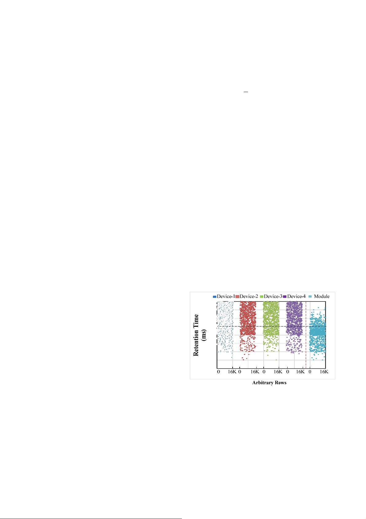
device integration on FGR DRAM. Fig. 3 shows the retention
time of four DRAM devices generated with our PV model. In
Fig. 3, each dot represents the retention time (y-axis) of one
particular row (x-axis) of one device in continuous physical row
addresses.
0
128
256
384
512
640
768
896
1024
Refresh Interval
Abitrary Devices
系列1 系列2 系列3 系列4 系列5
Fig.3 Retention time of rows in four separate devices and the composed rank
In Fig. 3, each of the devices has 16K rows with varying
retention time denoted by scattered points. If such four devices
are becoming one DIMM, four rows belonging to the same
address but different devices will become a “full” row.
Similarly, in Fig.3, the “module” region shows the retention
time of all the 16K corresponding “full” rows after the four
devices are bound together as one DIMM. Originally, the four
devices have a great potential of refresh reduction with FGR
control since most of their rows are distributed in high retention
region shown in Fig. 3. However, they manifest as a leaky


