ADS1282高精度模拟到数字转换器技术手册
需积分: 18 97 浏览量
更新于2024-07-17
收藏 1.64MB PDF 举报
"ADS1282手册 - AD1282英文手册,详细完整版"
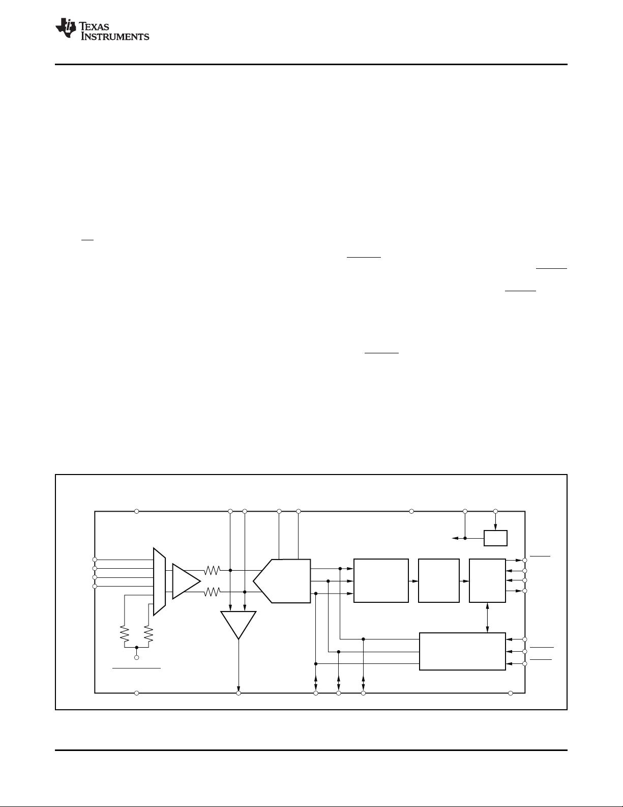
本文将详细讨论ADS1282,这是一个高分辨率、高精度的单芯片模拟到数字转换器(ADC),广泛应用于能源勘探和地震监测等对性能要求极高的环境。ADS1282集成了一款低噪声可编程增益放大器(PGA)和双通道输入多路复用器(MUX),以提供卓越的噪声和线性性能。
**主要特点:**
1. **高分辨率**:拥有130dB的信噪比(SNR),在250SPS(样本每秒)时,体现了其出色的信号质量。
2. **高精度**:总谐波失真(THD)低至-122dB,表明了其在信号转换过程中的高保真度。同时,积分非线性(INL)仅为0.5ppm,意味着在宽动态范围内具有极高的线性度。
3. **低噪声PGA**:内置的低噪声PGA可以增强弱信号的检测能力,同时降低噪声干扰。
4. **双通道输入多路复用器**:允许用户选择两个不同的输入信号进行数字化处理,增加了系统灵活性。
5. **四阶δ-Σ调制器**:这种内在稳定的调制器设计提供了快速响应和出色的噪声抑制性能。
**技术细节:**
ADS1282的核心是一个四阶δ-Σ调制器,这种调制方式以其自稳定性而闻名,能够有效减少量化噪声并提高转换精度。调制器的输出经过可编程数字滤波器处理,进一步优化了噪声性能和信号恢复。
**接口与控制:**
- **SPI接口**:ADS1282通过SPI(串行外围接口)与微控制器通信,进行配置和数据传输。
- **校准控制**:设备支持校准功能,以确保在整个工作温度和电源电压范围内保持高精度。
- **时钟(CLK)**:外部时钟输入用于同步ADC的操作。
- **电源引脚(AVDD, AVSS, DVDD, DGND)**:这些引脚提供模拟和数字电源,确保ADC正常工作。
- **控制引脚(DRDY, RESET, PWDN)**:DRDY指示转换完成,RESET用于复位设备,PWDN是待机模式控制。
**应用与支持:**
ADS1282产品文件夹包含了样片购买、技术文档、工具软件以及支持和社区资源,方便开发者获取更多信息和开发支持。
**总结:**
ADS1282是一款高度集成的ADC,其高性能特性使其成为需要精确测量和低噪声操作的应用的理想选择。结合其强大的PGA和MUX功能,它能够在能源勘探和地震监测等对数据质量和实时性有严格要求的领域发挥关键作用。通过SPI接口,开发者可以轻松地对其进行配置和控制,以满足具体应用需求。
0.50
0.46
GainError(%)
8
6
4
2
0
Occurrences
0.42
0.38
0.02
0.34
0.30
0.26
0.18
0.22
0.14
Worst-CaseGainMatchRelativePGA=1(25Units)
0.10
0.06
-15
-14
GainDrift(ppm/ C)°
90
80
70
60
50
40
30
20
10
0
Occurrences
-13
-12
5
-11
-10
-9
PGA=1,2,4
PGA=8,64
-7
-8
-6
25UnitsBasedon+20 CIntervals
OvertheRangeof 40 Cto+85 C
°
° °-
PGA=32
PGA=16
4
3
2
1
0
-5
-4
-3
-2
-1
-0.10
-0.08
OffsetDrift( V/ C)m °
90
80
70
60
50
40
30
20
10
0
Occurrences
-0.06
-0.04
0.10
-0.02
0
0.02
PGA=8
PGA=1
0.06
0.04
0.08
25UnitsBasedon
+20 CIntervals
OvertheRangeof
40 Cto+85 C
°
° °-
-1.2 -1.1
Gain Error (%)
10
8
6
4
2
0
Occurrences
-1.0 -0.9 -0.3-0.8 -0.7 -0.6
25 Units
-0.4-0.5
1.0 1.5
f (MHz)
CLK
30
25
20
15
10
5
0
Power (mW)
2.0 2.5 4.53.0 3.5 4.0
-100 -80
Offset( V)m
30
25
20
15
10
5
0
Occurrences
-60 -40 100-20 0 20
25Units
PGA=8
PGA=1
806040
ADS1282
SBAS418I –SEPTEMBER 2007–REVISED MARCH 2015
www.ti.com
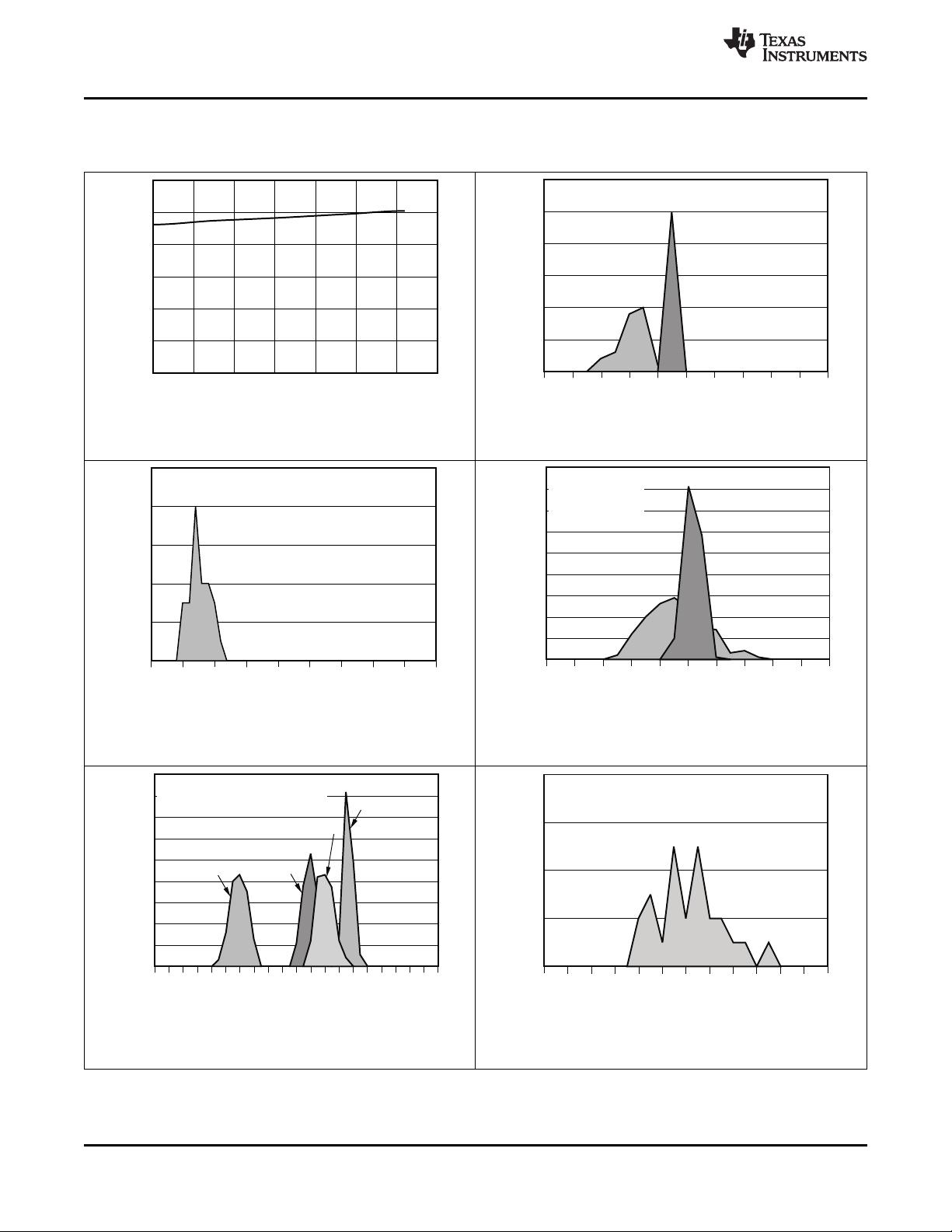
Typical Characteristics (continued)
At +25°C, AVDD = +2.5V, AVSS = –2.5V, f
CLK
= 4.096MHz, VREFP = +2.5V, VREFN = –2.5V, DVDD = +3.3V, PGA = 1,
CAPN – CAPP = 10nF, and f
DATA
= 1000SPS, unless otherwise noted.
Figure 19. Power vs Clock Frequency Figure 20. Offset Histogram
Figure 21. Gain Error Histogram
Figure 22. Offset Drift Histogram
Figure 23. Gain Drift Histogram
Figure 24. Gain Match Histogram
10 Submit Documentation Feedback Copyright © 2007–2015, Texas Instruments Incorporated
Product Folder Links: ADS1282
剩余53页未读,继续阅读
439 浏览量
618 浏览量
548 浏览量
2009-04-18 上传
2021-09-30 上传
381 浏览量
425 浏览量

forever_zl
- 粉丝: 0
- 资源: 1
 我的内容管理
展开
我的内容管理
展开


最新资源
- 基于Cordova + Framework7 + React + Webpack构建混合App.zip
- CoronaGame_front
- 无线传感网络节点能耗模型.zip
- 蓝色扁平化商务工作汇报图表下载PPT模板
- ember-bootstrap-controls:一个Ember组件库,它使用Bootstrap4表单并输入样式和html
- PWABuilder-CLI:用于应用程序生成的Node.js工具
- XY轴点焊机_三菱伺服_
- 毕业设计,基于人脸识别的智能家居控制系统.zip
- rust-reference-book:中文版的Rust参考
- assignment-problem:匈牙利方法的分配问题
- 微立体建筑行业工作汇报图表大全PPT模板
- 电脑使用时间管理 ManicTime-4.3.rar
- firebase-firestore-lite:浏览器的轻量级云Firestore库
- bouquins:calibre 电子书管理器的 Web 前端
- MFC中修改Button控件字体、字体大小、背景色、背景图片
- Baymin是一个基于Android系统开发的可以用于语音聊天的智能机器人,它能够陪你聊天,帮你查天气,查路线、车票.zip
