704 CHINESE OPTICS LETTERS / Vol. 6, No. 10 / October 10, 2008
Photonic crystal waveguides and their applications
Invited Paper
Yidong Huang (
ÀÀÀ
), Xiaoyu Mao (
fff
¡¡¡
), Chao Zhang (
ÜÜÜ
), Lei Cao (
ùùù
[[[
),
Kaiyu Cui (
www
mmm
), Wei Zhang (
ÜÜÜ
), and Jiangde Peng (
$$$
)
State Key Laboratory of Integrated Optoelectronics, Department of Electronic Engineering,
Tsinghua University, Beijing 100084
Received June 10, 2008
Two-dimensional (2D) slab photonic crystal waveguides (PCWGs) on silicon-on-insulator (SOI) wafer were
designed and fabricated. Full photonic band gap, band gap guided mode, and index guided mode were
observed by measuring the transmission spectra. Mini-stop-bands in the PCWG were simulated with
different structure parameters. Coupling characteristics of PCWG were investigated theoretically consid-
ering the imperfections during the fabrication process. It was found that suppressing power reservation
effect can realize both short coupling length and high coupling efficiency.
OCIS codes: 160.5298, 230.7370.
doi: 10.3788/COL20080610.0704.
Photonic crystal (PC) has been focused o n since it was
proposed by Yablonovitch
[1]
and John
[2]
in 1987, as it can
provide a novel way to guide, control, and manipulate
the photons. In various P C structures, two-dimensional
(2D) PC slabs, which a re normally ma de by periodically
patterning an array of air holes in high refractive index
materials slabs, have rec eived considerable a ttention in
recent years
[3−6]
for its in-plane band-gap and compati-
ble fabrication method with the traditional semiconduc-
tor wafer process. Inducing a line defect to the slab,
PC would form a band gap confinement PC waveguide
(PCWG)
[7]
, which is the fundamental part of most PC
based devices
[8]
.
This paper reviews our present research work on the
PCWG. A 2D slab PCWG on silicon-on-insulator (SOI)
wafer was designed a nd fabricated with traditiona l str ipe
waveguides for joint. By measuring the trans mission
sp e ctra, full photonic band gap, band gap guided mode,
and index guided mode were observed near 1.55 µm.
Mini-stop-bands in the PCWG were discussed with
different structure parameters. It is found that their
centre frequency is very sensitive to the refractive in-
dex of the substance filled in the holes of P C . Coupling
characteristics of PCWG were investigated theoretically
by considering the imperfections during the fabrication
process. It was found that s uppressing power reservation
effect can realize both short coupling length and high
coupling efficiency.
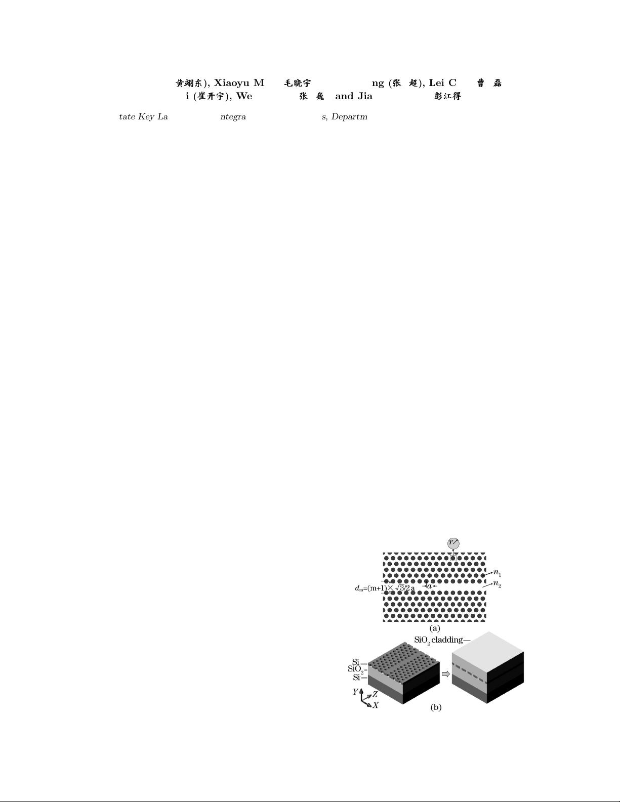
Figure 1(a) shows the simulation model of the PCWG.
The refractive index of the background and the substance
filled in the holes is n
2
and n
1
, res pectively. The lattice
constant is a, the radius of the air holes is r, and r/a is
taken as a key s tructure factor for the following discus-
sions because it decides the air-filling factor of the PCs
f ∝ (r/a)
2
. We designed the PCWG by plane wave
expansion method and finite-difference time-domain
(FDTD) simulation to ens ure the band gap g uided mode
around the wavelength of 1.5 µm. Here, s iz e enlarge was
considered because hole size would be enlarged during
the fabrication. Line defect PCWGs along Γ- K direction
were fabricated. Figure 1(b) shows the structur e . SOI
wafer with a 200-nm-thick silicon film on the top and a
3000-nm-thick buried SiO
2
layer was used. Using a ZEP-
520A resist mask, PC pattern was generated perfectly
by electron beam (EB) lithography. Then an induc-
tively coupled plasma (ICP) dry etching was employed
to transfer the pattern to the silicon film. After remov-
ing the resist mask, a 600-nm-thick SiO
2
cover layer was
deposited on the surface to form a symmetry SiO
2
clad
structure for reducing the radiation loss in the vertical
direction. Finally, we ground the wafer to about 100-µm
thick, and cleaved them into ab out 1 mm-long samples
for measurement. We removed some sample’s upper SiO
2
cover layer by HF etching to verify the size and shape
of the holes by scan electron micros c op e (SEM). Figure
2 are the SEM pictures for a slab PC without line de-
fect and a line defect PCWG along Γ-K direction. The
period a and the radius r of the PC are 380 nm and 90
nm, re spec tively. The coupling loss between a tapered
fiber and a stripe waveguide was measured. For tapere d
fiber with 1.7-µm fo c us diameter, we found that a 2-µm
wide waveguide had the lowest coupling loss of −7 dB
per facet. Therefore 2-µm-wide waveguide was used for
Fig. 1. (a) Simulation model and (b) symmetry SiO
2
clad
structure.
1671-7694/2008/100704-05
c
2008 Chinese Optics Letters


