DS90CR215, DS90CR216
www.ti.com
SNLS129D –MARCH 1999–REVISED APRIL 2013
Transmitter Switching Characteristics (continued)
Over recommended operating supply and −40°C to +85°C ranges unless otherwise specified
Symbol Parameter Min Typ Max Units
TPPos0 Transmitter Output Pulse Position for Bit0
(2)
f = 66 MHz −0.4 0 0.3 ns
(Figure 20)
TPPos1 Transmitter Output Pulse Position for Bit1 1.8 2.2 2.5 ns
TPPos2 Transmitter Output Pulse Position for Bit2 4.0 4.4 4.7 ns
TPPos3 Transmitter Output Pulse Position for Bit3 6.2 6.6 6.9 ns
TPPos4 Transmitter Output Pulse Position for Bit4 8.4 8.8 9.1 ns
TPPos5 Transmitter Output Pulse Position for Bit5 10.6 11.0 11.3 ns
TPPos6 Transmitter Output Pulse Position for Bit6 12.8 13.2 13.5 ns
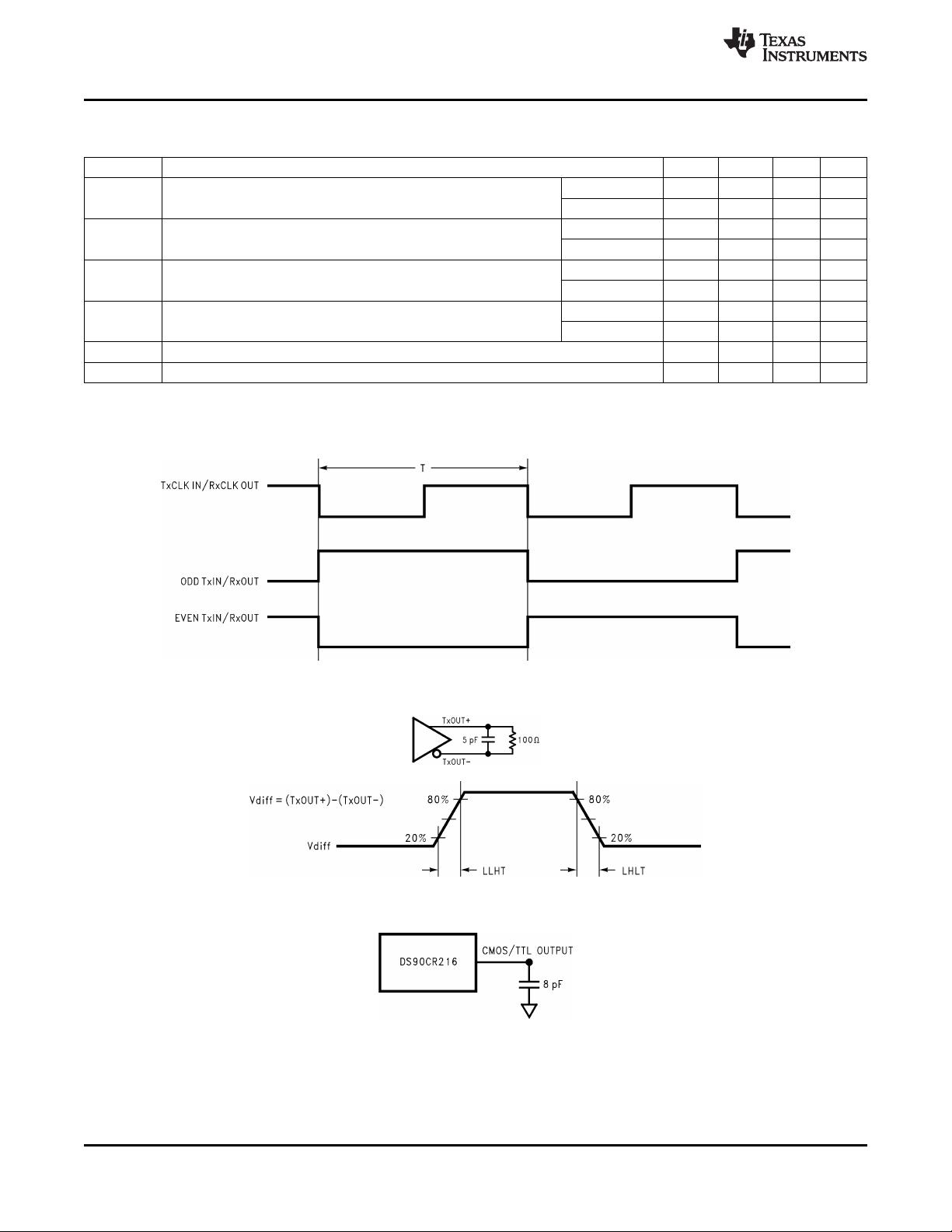
TCIP TxCLK IN Period (Figure 10) 15 T 50 ns
TCIH TxCLK IN High Time (Figure 10) 0.35T 0.5T 0.65T ns
TCIL TxCLK IN Low Time (Figure 10) 0.35T 0.5T 0.65T ns
TSTC TxIN Setup to TxCLK IN (Figure 10) 2.5 ns
THTC TxIN Hold to TxCLK IN (Figure 10) 0 ns
TCCD TxCLK IN to TxCLK OUT Delay @ 25°C,V
CC
=3.3V (Figure 12) 3 3.7 5.5 ns
TPLLS Transmitter Phase Lock Loop Set (Figure 14) 10 ms
TPDD Transmitter Powerdown Delay (Figure 18) 100 ns
(2) The min. and max. limits are based on the worst bit by applying a −400ps/+300ps shift from ideal position.
Receiver Switching Characteristics
Over recommended operating supply and −40°C to +85°C ranges unless otherwise specified
Symbol Parameter Min Typ Max Units
CLHT CMOS/TTL Low-to-High Transition Time (Figure 7) 2.2 5.0 ns
CHLT CMOS/TTL High-to-Low Transition Time (Figure 7) 2.2 5.0 ns
RSPos0 Receiver Input Strobe Position for Bit 0
(1)
(Figure 21) f = 40 MHz 1.0 1.4 2.15 ns
RSPos1 Receiver Input Strobe Position for Bit 1 4.5 5.0 5.8 ns
RSPos2 Receiver Input Strobe Position for Bit 2 8.1 8.5 9.15 ns
RSPos3 Receiver Input Strobe Position for Bit 3 11.6 11.9 12.6 ns
RSPos4 Receiver Input Strobe Position for Bit 4 15.1 15.6 16.3 ns
RSPos5 Receiver Input Strobe Position for Bit 5 18.8 19.2 19.9 ns
RSPos6 Receiver Input Strobe Position for Bit 6 22.5 22.9 23.6 ns
RSPos0 Receiver Input Strobe Position for Bit 0
(2)
(Figure 21) f = 66 MHz 0.7 1.1 1.4 ns
RSPos1 Receiver Input Strobe Position for Bit 1 2.9 3.3 3.6 ns
RSPos2 Receiver Input Strobe Position for Bit 2 5.1 5.5 5.8 ns
RSPos3 Receiver Input Strobe Position for Bit 3 7.3 7.7 8.0 ns
RSPos4 Receiver Input Strobe Position for Bit 4 9.5 9.9 10.2 ns
RSPos5 Receiver Input Strobe Position for Bit 5 11.7 12.1 12.4 ns
RSPos6 Receiver Input Strobe Position for Bit 6 13.9 14.3 14.6 ns
RSKM RxIN Skew Margin
(3)
(Figure 22) f = 40 MHz 490 ps
f = 66 MHz 400 ps
RCOP RxCLK OUT Period (Figure 11) 15 T 50 ns
RCOH RxCLK OUT High Time (Figure 11) f = 40 MHz 6.0 10.0 ns
f = 66 MHz 4.0 6.1 ns
(1) The min. and max. are based on the actual bit position of each of the 7 bits within the LVDS data stream across PVT.
(2) The min. and max. limits are based on the worst bit by applying a −400ps/+300ps shift from ideal position.
(3) Receiver Skew Margin is defined as the valid data sampling region at the receiver inputs. This margin takes into account for transmitter
pulse positions (min and max) and the receiver input setup and hold time (internal data sampling window). This margin allows LVDS
interconnect skew, inter-symbol interference (both dependent on type/length of cable), and clock jitter less than 250 ps.
Copyright © 1999–2013, Texas Instruments Incorporated Submit Documentation Feedback 5
Product Folder Links: DS90CR215 DS90CR216


