EMI Analysis of TFT-LCD Driver IC
Sung-Pil Choi, Jae Wook Kwon, Kye Eon Chang, Jin Tae Kim
1
, Min Koo Han
2
(List authors on this line using 12 point Times New Roman - use a second line if necessary)
1
Samsung Electronics Co., Ltd.LSI Research-BD, San #16 Banwol-Dong Taean-Gu, Hwasung-City, South Korea
E-mail : sungpil.choi@samsung.com
2
Department of Electrical Engineering & Computer Science, Seoul National University, South Korea
Abstract — In this paper, design for EMC of LCD Driver
IC is proposed. By the analysis with package parasitic
parameters and EMC test pattern, local power/ground noise
in LCD Driver IC simulated. As a result of analysis, design
for lower peak of EMI spectrum and design for lower mean
level of that is proposed at the same time.
In addition, decoupling cap with CMOS process can
decrease EMI spectrum without any further mask. The
analysis of the proposed design shows that LCD Driver IC
can be alternatives for TFT-LCD EMC solution. It is
because LCD Driver IC is nearly irrelevant to LCD module
whereas source PCB should be redesigned separately
according to the size and resolution of LCD panel.
The experimental result shows that the proposed design
methodology for LCD Drier IC can successfully decrease
EMI spectrum of LCD module.
I. I
NTRODUCTION
The LCD monitor requires low EMI characteristics for
Home appliances. Under FCC regulations, The LCD
monitor violates EMC specification more frequently than
CRT monitor because LCD module has many high-speed
and high-frequency electronic devices such as time-
controller(T-CON) or LCD Driver ICs(below LDI). The
clock frequency of data interface for these devices is
several hundreds of kilohertz, these devices as EMI noise
sources cause EMC problem in LCD module.
The method for EMC solution is divided by IC level,
plane level and system level. In the case of LCD module,
the plane level approach is general method in the industry.
TFT-LCD module is constituted of LCD panel, main
PCB(SMPS), source PCB(T-CON), and other else. EMC
problem of LCD module is fixed traditionally by the
amendment of source PCB because ICs in source PCB
operate at high frequency. It depends on attaching or
detaching beads and bypass/decoupling capacitors.
However, this method is restricted to the specific display
resolution or LCD panel size because source PCB of LDI
module is designed separately according to LCD panel
size. Whereas source PCB, LCD Driver IC is nearly
irrelevant to LCD module specification.
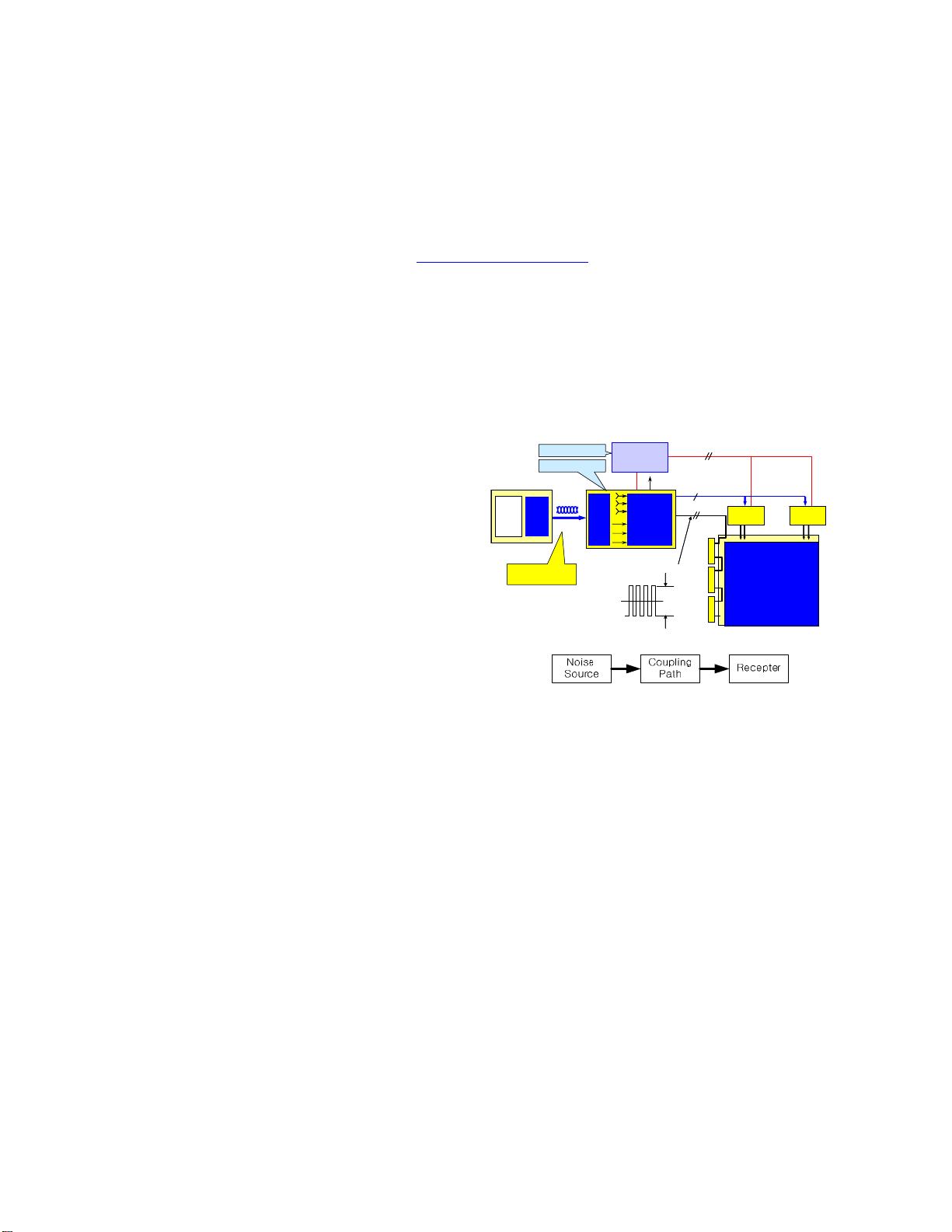
Fig.1(a) shows Data interface and block connection
diagram between PC and LCD monitor. T-CON and
LCD can deserve the noise source in the LCD monitor.
Data bus and LCD module can be coupling path.[1]
This paper approaches the EMI problem of TFT-LCD
module by IC level, especially LDI. First, the analytic
strategy of EMI with the consideration of LDI will be
described. Second, simulated power/ground noise
reduction with extracted package parameter will be
presented. Third, short current with output polarity
transition will be surveyed. Finally, the measured EMI
spectrum of LCD module will be compared to whether
these two enhancements are adapted
LCD Panel
Gray Scale Voltage & Vcom
Control Signal
LVDS
Tx
RGB Data & Clock
LVDS
Rx
Timing
Controller
R
G
B
Vsync
Hsync
Control
Graphic
Controller
Source Driver
DC-DC
Gamma
Vcom
GUI
. . .
Source Driver
TTL
3.3V
Gate Driver IC’s
(340mV)
LVDS Input
(Low EMI Bus)
Analog Part
Digital Part
LCD Panel
Gray Scale Voltage & Vcom
Control Signal
LVDS
Tx
RGB Data & Clock
LVDS
Rx
Timing
Controller
R
G
B
Vsync
Hsync
Control
Graphic
Controller
Source Driver
DC-DC
Gamma
Vcom
GUI
. . .
Source Driver
TTL
3.3V
Gate Driver IC’s
(340mV)
LVDS Input
(Low EMI Bus)
Analog Part
Digital Part
(a)
(b)
Fig. 1. (a)Data Interface and structure diagram between PC and
LCD monitor (b) EMI factor
II. ANALYSIS
OF
LCD
DRIVER
IC
A. Structure of LDI
LDI received the display data with interface of
RSDS(Reduced Swing Differential Signaling) or
LVDS(Low Voltage Differential Signaling) of which the
clock frequency is 85MHz ૫ 170MHz. The display data
is converted to DAC after parallelization as shown at
Fig.2. Analog signal is buffered by voltage follower in
order to drive LCD panel. Each load of data line at LCD
panel is about several hundreds of pico farads(pF). In
short, LDI doesn’t use standardized TTL I/O buffer, IBIS
model which is waveform characterization format of IC
cannot be represented precisely in LDI domain.
Hence, SI/PI analysis is more suitable for not I/O buffer
but inner blocks at design for EMC. Because inner blocks
of LDI is composed with the array of the identical
structure, short current level induced by clock transition
is very high. Power/Ground bouncing induced from short
17th International Zurich Symposium on Electromagnetic Compatibility, 2006
606
Authorized licensed use limited to: XIDIAN UNIVERSITY. Downloaded on May 13,2010 at 13:19:51 UTC from IEEE Xplore. Restrictions apply.


