694 IEEE JOURNAL OF QUANTUM ELECTRONICS, VOL. 45, NO. 6, JUNE 2009
Optimum Design for 160-Gb/s All-Optical
Time-Domain Demultiplexing Based on Cascaded
Second-Order Nonlinearities of SHG and DFG
Jing Shen, Song Yu, Wanyi Gu, and Jian Quan Yao
Abstract—All-optical time-domain demultiplexing based on
cascaded second-order nonlinearities of second-harmonic genera-
tion and difference-frequency generation in quasi-phase-matched
periodically poled lithium niobate waveguides is discussed in order
to maximize conversion efficiency and control crosstalk under
the given level. The three parameters, including the waveguide
length, clock pulsewidth, and clock offset, are investigated care-
fully and comprehensively. The concepts of maximum waveguide
length, maximum clock pulsewidth, and optimal clock offset are
defined, and their theoretical expressions are derived for the
demultiplexing from 160 to 10 Gb/s. The results calculated from
the theoretical expressions are well-consistent with those from
the numerical simulation. For two kinds of practical situations,
the waveguide length or the clock offset being given, an optimum
scheme is proposed to determine the other two parameters readily.
The maximum conversion efficiency can therefore be achieved
while the quality of the converted wave is sufficient for the prac-
tical situations.
Index Terms—All-optical time-domain multiplexing (OTDM),
cascaded second-order nonlinearities, conversion efficiency,
crosstalk, difference-frequency generation (DFG), periodically
poled lithium niobate (PPLN), quasi-phase-matching (QPM),
second-harmonic generation (SHG).
I. INTRODUCTION
A
LL-OPTICAL time-domain multiplexing (OTDM)/de-
multiplexing is an important function in high-speed
OTDM networks and signal processing systems to elimi-
nate the demands on optical--electrical--optical conversions.
Many efforts have been paid to fulfill this function using dif-
ferent methods [1]–[5]. Based on the cascaded second-order
nonlinearities of second-harmonic generation (SHG) and differ-
ence-frequency generation (DFG), periodically poled lithium
niobate (PPLN) waveguide has many advantages in wavelength
conversion, such as high efficiency, ultrafast response, low
noise, integration compatibility [6]–[13]. Therefore, PPLN
Manuscript received April 27, 2008; revised September 16, 2008. Current
version published May 15, 2009. This work was supported by National Science
Foundation under Grant 60837004 and Grant 60602004, Hi-Tech Research and
Development Program of China under Grant 2009AA01Z220, and China Post-
doctoral Science Foundation.
J. Shen, S. Yu, and W. Gu are with Key Laboratory of Optical Communi-
cation and Lightwave Technologies, Ministry of Education, Beijing Univer-
sity of Posts and Telecommunications (BUPT), Beijing 100876, China (e-mail:
jing76iver@gmail.com; yusong@bupt.edu.cn; wyg@bupt.edu.cn).
J. Q. Yao is with Tianjin University, Tianjin 300072, China (e-mail:
jqyao@tju.edu.cn).
Digital Object Identifier 10.1109/JQE.2009.2013147
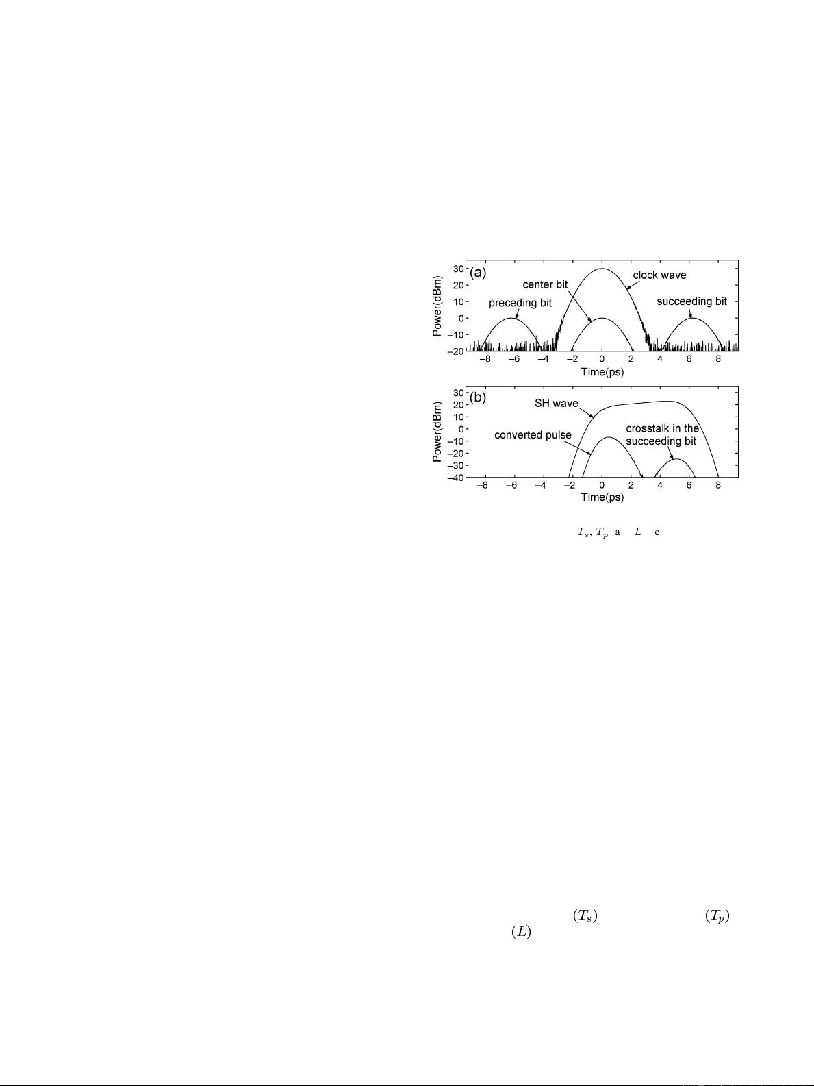
Fig. 1. Waveforms without optimization. (a) Input clock and signal.
(b) Output SH and converted wave.
T
,
T
, and
L
are set at 0 and 2 ps and
2 cm, respectively.
is a good choice to be used in all-OTDM/demultiplexing by
employing SHG and DFG. Some experiments [1]–[5] and
analyses [15]–[18] have been reported recently.
The focus of this paper intend to discuss the optimum design
of the demultiplexer based on PPLN waveguides. Two schemes
are alternative to arrange signal wave and clock wave according
to which wave is involved into the SHG [17], [18]. In scheme
I, as shown in Fig. 1, the frequency of the clock wave is dou-
bled through SHG, and subsequently, the generated second-har-
monic (SH) wave acts with the signal wave through DFG. The
converted wave would have the same bit rate as the clock wave
and carry the code information from the required channel of the
signal wave. In scheme II, it is the signal not the clock that is
involved in the SHG [17], [18]. Commonly, scheme I is adapted
in most experiments and numerical simulations. For example,
demultiplexing from 160 to 10 Gb/s has been demonstrated by
employing scheme I [4]. The objective of this paper is to en-
hance the conversion efficiency and control the crosstalk by op-
timizing the parameters of scheme I. The methods developed in
scheme I can also be employed into scheme II.
In scheme I, clock offset
, clock pulsewidth , and
waveguide length
are three critical parameters to the conver-
sion efficiency and crosstalk of the converted wave. As shown
in Fig. 1(a), the required channel of the signal wave is called
center bit, and its two adjacent bits are called preceding bit and
succeeding bit, respectively. Because of the group-velocity mis-
match (GVM), the SH pulse would be widened and fall behind
0018-9197/$25.00 © 2009 IEEE
Authorized licensed use limited to: BEIJING UNIVERSITY OF POST AND TELECOM. Downloaded on May 20, 2009 at 04:53 from IEEE Xplore. Restrictions apply.


