T
oday’s SOC (system-on-chip) designs have dozens
of clocks, many of which are asynchronous. This
design approach facilitates the convergence of dig-
ital-audio, video, wireless, and networking applica-
tions in a single chip. CDCs (clock-domain cross-
ings) can cause difficult-to-detect functional fail-
ures in SOCs involving multiple asynchronous clocks. Simula-
tion and static-timing analysis often do not detect issues such
as metastability and the coherency of correlated signals’ CDCs;
as a result, these issues often end up as bugs in silicon. Unfortu-
nately, most relevant literature does not adequately cover some
of these critical CDC issues, and designers learn about them
only after making costly mistakes. Two of the most common
and critical issues involving CDCs are improper sequencing of
data/enable in enable-based synchronization and data coher-
ency due to the convergence of signals.
EnablE-basEd synchronization
A receiver flip-flop output can become metastable if it vio-
lates the data/reset setup-and-hold times. This scenario can
arise when the transmitter—the source of data—and the re-
ceiver flip-flop are in asynchronous-clock domains. To avoid
such issues, designers use synchronizers that isolate metasta-
bility and deliver a clean signal to the downstream logic. A
synchronizer can be a simple double flip-flop. Designers com-
monly use this technique for a control signal’s CDCs. In a data
transfer across clock domains, the data is first set up; then, a
control signal that synchronizes with the destination domain
travels to the destination to enable data capture. Although
this data-transfer technique across clock domains is a common
and proven technique, it involves pitfalls that require special
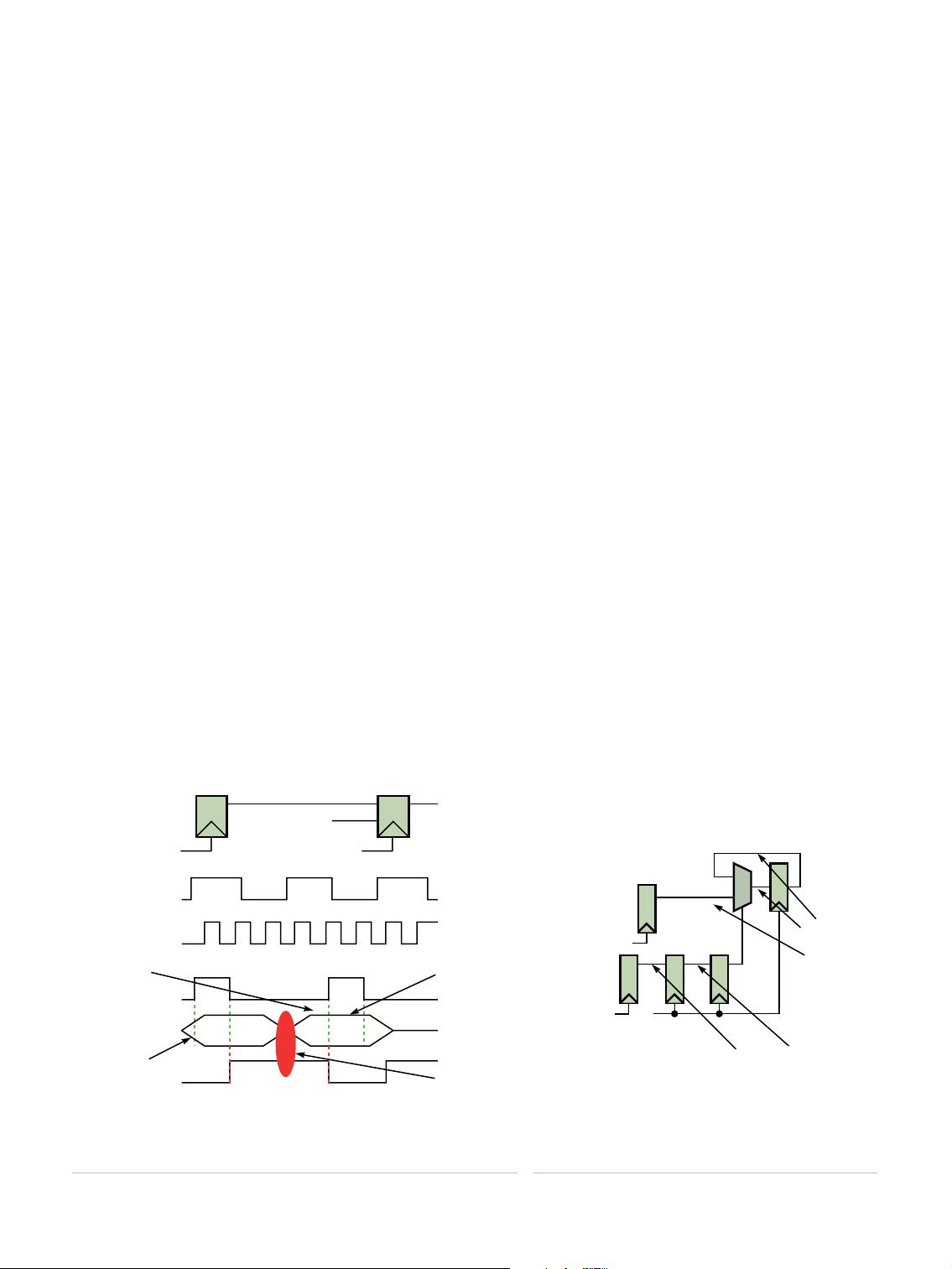
attention. This technique relies on data to be stable when you
assert an enable (Figure 1).
Having too low a margin between the data you are set-
ting up and the enable you are asserting may corrupt the data
transfer. A good way to prevent such problems is to design a
full handshake when you set up the data. In this approach, you
assert and synchronize the request in the destination domain
and adequately assert an acknowledge to let the next data load
occur. This approach might add a few cycles of latency, but it
avoids functional failures.
Glitches are other sources of worry across clock domains.
Typically, any combinational logic may be subject to short-
lived glitches. These issues are generally harmless because
they resolve themselves when you activate the next clock
edge. Although these issues are not problematic for synchro-
nous transfers, a glitch may occur with asynchronous cross-
ings if you activate a destination clock. The design may there-
fore receive a glitch as a pulse, causing a functional failure.
For this reason, it is important to avoid using any combi-
national logic that may cause glitches on a CDC path. You
b y s h ak e r s a r wa r y a n d s au r a bh V e r m a • at r e nta I n c
Critical clock-domain-
crossing bugs
AWARENESS OF CDC ISSUES, ALONG WITH THE USE
OF GOOD DESIGN PRACTICES AND PROVEN EDA TOOLS
FOR CDC VERIFICATION, CAN AVOID COSTLY SILICON
RE-SPINS AND SIGNIFICANTLY IMPROVE TIME TO MARKET.
STEVE EDN080320MS4271 FIGURE 1
ADEQUATE
MARGIN:
DATA WILL
BE PROPERLY
CAPTURED
SHORT OR
NO MARGIN:
DATA MAY
GET LOST
INCORRECT
DATA/ENABLE
SEQUENCING
PROPER
DATA/ENABLE
SEQUENCING
D
E
E
CLOCK 2CLOCK 1
CLOCK 1
D
E
CLOCK 2
Figure 1 In a data transfer across clock domains, the data must be stable
when enable is asserted. Too short of a margin between data setup and
enable assertion can result in data corruption.
april 3, 2008 | EDN 55
STEVE EDN080320MS4271 FIGURE 2
DO NOT COMBINE
LOGIC ON
CONTROL PATH
AVOID
COMBINING
LOGIC ON
DATAPATH
CLOCK 2
CLOCK 1
CLOCK 1
Figure 2 A good design practice is to avoid using any
logic, except the recirculation-multiplexer logic, which is
part of the enable flip-flop, on the datapath CDCs.


