"DDR2内存条PCB布线规范及设计指南"
需积分: 9 107 浏览量
更新于2023-12-15
收藏 612KB PDF 举报
DDR2内存条的PCB布线规范是非常重要的,它涉及到板载设计和性能的最大化。本文总结了Freescale Semiconductor公司发布的关于DDR2内存条的PCB布线规范,旨在帮助设计师避免在多种内存拓扑结构下出现的板级问题,并为设计师提供最大的灵活性。
DDR2内存条的PCB布线规范是基于Freescale Semiconductor公司内部平台的设计经验总结而来的,该公司是一家在半导体和嵌入式解决方案领域拥有丰富经验的领军企业。因此,这些规范可以被认为是可靠和经过验证的。
首先,布线规范的目的是最小化与板级设计相关的问题。DDR2内存条的PCB布线是非常复杂的,需要符合一定的规范,否则可能导致性能下降甚至导致系统不稳定。因此,遵循布线规范是确保内存子系统正常工作的关键。
其次,布线规范还要求在提供最大的灵活性给设计师的同时保持兼容性。这意味着设计师可以根据需要进行定制化的布线,以适应不同的系统配置和应用需求。同时,这些规范还包括了一些通用的规则和建议,以确保布线的质量和稳定性。
根据布线规范,DDR2内存条的PCB布线需要考虑以下几个方面:
首先是地线和电源线的布线。地线和电源线是布线中最重要的部分,它们的稳定性直接影响到系统的性能和稳定性。因此,在布线过程中需要遵循一定的规则,如尽量缩短地线和电源线的长度,尽量减少回流路径的阻抗,保持地线和电源线的距离和平行性等。
其次是时钟线和信号线的布线。时钟线和信号线是传输数据的关键路径,它们的布线质量直接影响到系统的可靠性和性能。因此,在布线过程中需要注意时钟线和信号线的长度匹配,控制传输延迟,避免电磁干扰,减少电路噪音等。
另外,布线规范还提供了关于终端电阻、信号层分离、引脚分配和屏蔽等方面的具体建议。这些建议可以帮助设计师更好地进行DDR2内存条的PCB布线,以达到最佳的性能和稳定性。
需要注意的是,DDR2内存条的PCB布线规范是一项复杂的任务,需要设计师具备一定的经验和专业知识。因此,建议设计师在进行布线之前仔细阅读相关的文档和技术资料,并遵循布线规范进行设计。
综上所述,DDR2内存条的PCB布线规范是确保内存子系统正常工作的关键。遵循规范可以最小化与板级设计相关的问题,并在提供最大灵活性的同时保持兼容性。设计师需要注意地线和电源线的布线,时钟线和信号线的布线以及其他方面的具体建议。通过遵循布线规范,设计师可以实现DDR2内存条的最佳性能和稳定性。
Hardware and Layout Design Considerations for DDR2 SDRAM Memory Interfaces, Rev. 2
4 Freescale Semiconductor
Designer’s Checklist
24. Suggest routing order within the DDR2 interface:
1) Data, 2) Address/Command, 3) Control, 4) Clocks, and 5) Power
This order allows the clocks to be tuned easily to the other signal groups. It also assumes an open
critical layer on which clocks are freely routed.
25. Global items—
• Do not route any DDR2 signals overs splits or voids.
• Traces routed near the edge of a reference plane should maintain at least 30–40 mil gap to the
edge of the reference plane.
• Allow no more than 1/2 of a trace width to be routed over via antipad.
26. When routing the data lanes, route the outermost (that is, longest lane first) because this determines
the amount of trace length to add on the inner data lanes.
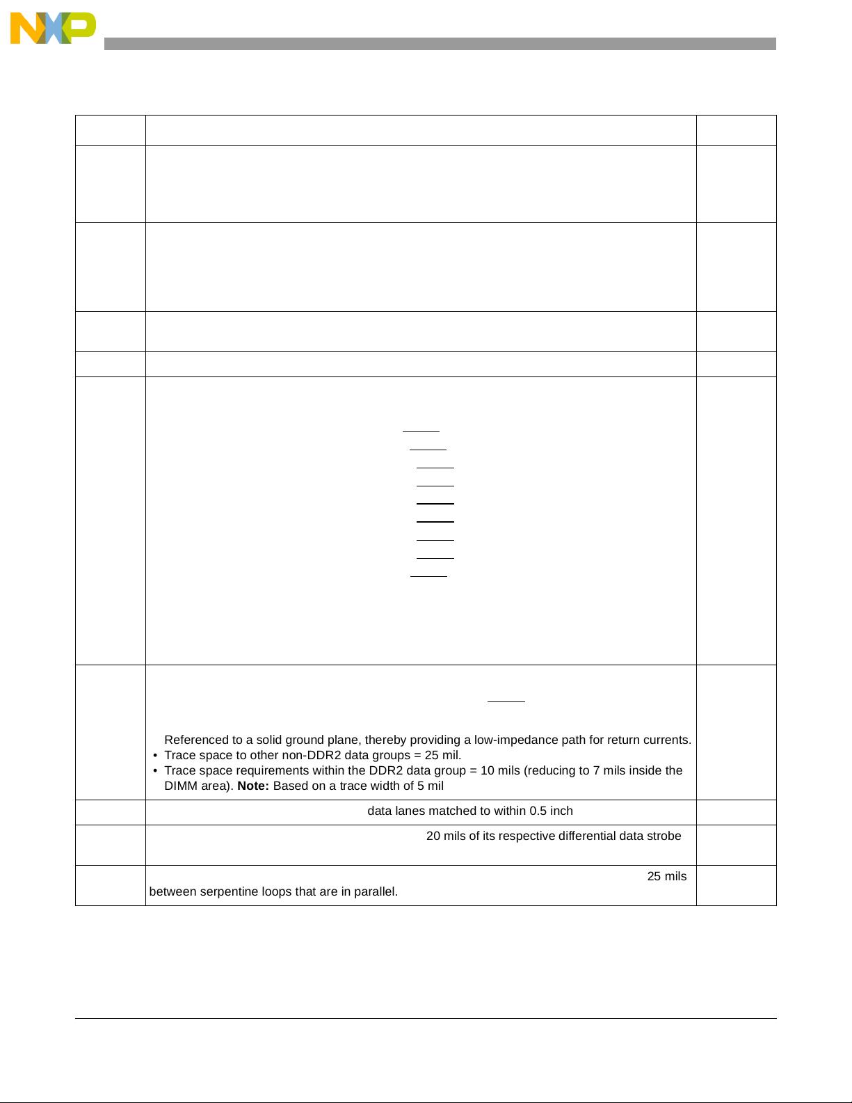
27. Are the clock pair assignments optimized to allow break-out of all pairs on a single critical layer?
28. The DDR2 data bus consists of 9 data byte lanes (assuming ECC is used). All signals within a given
byte lane should be routed on the same critical layer with the same via count.
Note: Some product implementations may only implement a 32-bit wide interface.
Byte Lane 0—MDQ(7:0), MDM(0), MDQS(0), MDQS
(0)
Byte Lane 1—MDQ(15:8), MDM(1), MDQS(1), MDQS
(1)
Byte Lane 2—MDQ(23:16), MDM(2), MDQS(2), MDQS
(2)
Byte Lane 3—MDQ(31:24), MDM(3), MDQS(3), MDQS
(3)
Byte Lane 4—MDQ(39:32), MDM(4), MDQS(4), MDQS
(4)
Byte Lane 5—MDQ(47:40), MDM(5), MDQS(5), MDQS
(5)
Byte Lane 6—MDQ(55:48), MDM(6), MDQS(6), MDQS
(6)
Byte Lane 7—MDQ(63:56), MDM(7), MDQS(7), MDQS
(7)
Byte Lane 8—MECC(7:0), MDM(8), MDQS(8), MDQS
(8)
To facilitate fan-out of the DDR2 data lanes (if needed), alternate adjacent data lanes onto different
critical layers? See Figure 1 and Figure 2.
Note: If the device supports ECC, Freescale highly recommends that the user implement ECC on
the initial hardware prototypes.
29. DDR2 data group—Impedance range and spacing
• Single-ended target Impedance = 50–60 Ω range (MDQ, MDM)
• Differential target impedance = 100–120 Ω range (MDQS, MDQS
) Note: Some product
implementations may support only the single-ended version of the strobe.
• Referenced to a solid ground plane, thereby providing a low-impedance path for return currents.
• Trace space to other non-DDR2 data groups = 25 mil.
• Trace space requirements within the DDR2 data group = 10 mils (reducing to 7 mils inside the
DIMM area). Note: Based on a trace width of 5 mil.
30. Across all DDR2 data lanes, are all the data lanes matched to within 0.5 inch?
31. Is each data lane properly trace matched to within 20 mils of its respective differential data strobe?
(Assumes highest frequency operation.)
32. When adding trace lengths to any of the DDR2 signal groups, ensure that there is at least 25 mils
between serpentine loops that are in parallel.
Table 1. DDR2 Designer’s Checklist (continued)
Item Description Yes/No
蛇形线间隔最少为25mils
DM和DQS和数据线差距在
20mils以内
不同组数据线差距在
500mils以内
数据线布线要求:
参考选实心地平面以提供
电流回流路径。
DDR和非DDR走线间距间隔
最低为25mils,在DDR内
部可以减少到10mils,在
DIMM(双列直插内存条)
区域可以减少到7mils
(线宽为5mils).
布线顺序:
1.数据线DQ、DM
2.地址&命令线Addr、Bank
Addr、RAS、CAS、WE
3.控制线CS、CKE、ODT
4.时钟线Clock_P/N
5.电源线
总体要求:
1.走线不能断裂
2.距离工作区边缘至少需
要30-40mils
3.和via电隔离区域至少
距离1/2线宽
最外圈的走线作为基准,
决定了整体的走线长度
剩余15页未读,继续阅读
2010-05-29 上传
点击了解资源详情
2022-01-13 上传
2010-12-11 上传
2022-05-16 上传
2013-08-13 上传
2014-06-04 上传

xuanwo17
- 粉丝: 0
- 资源: 2
 我的内容管理
展开
我的内容管理
展开


最新资源
- Angular实现MarcHayek简历展示应用教程
- Crossbow Spot最新更新 - 获取Chrome扩展新闻
- 量子管道网络优化与Python实现
- Debian系统中APT缓存维护工具的使用方法与实践
- Python模块AccessControl的Windows64位安装文件介绍
- 掌握最新*** Fisher资讯,使用Google Chrome扩展
- Ember应用程序开发流程与环境配置指南
- EZPCOpenSDK_v5.1.2_build***版本更新详情
- Postcode-Finder:利用JavaScript和Google Geocode API实现
- AWS商业交易监控器:航线行为分析与营销策略制定
- AccessControl-4.0b6压缩包详细使用教程
- Python编程实践与技巧汇总
- 使用Sikuli和Python打造颜色求解器项目
- .Net基础视频教程:掌握GDI绘图技术
- 深入理解数据结构与JavaScript实践项目
- 双子座在线裁判系统:提高编程竞赛效率
