优化Buck转换器PCB布局技巧
下载需积分: 44 | PDF格式 | 625KB |
更新于2024-08-04
| 125 浏览量 | 举报
"BUCK dcdc PCB layout 技术指南"
在设计开关电源集成电路时,PCB布局与电路设计同等重要。适当的布局可以避免由电源电路引起的各种问题,如输出和开关信号叠加产生的噪声增加、稳压器性能下降以及系统稳定性不足。本应用笔记将深入探讨BUCK降压转换器的PCB布局技术。
1. 主要电流路径
在BUCK转换器电路中,电流路径的设计至关重要。图1-a展示了当开关元件Q1导通时的主要电流流动路径。红色线条表示主电流流经的方向。C BYPASS 是一个高频旁路电容,用于滤波,而C IN 是大容量电容,主要在开关元件Q1导通时提供大部分陡峭的电流波形。
图1-b描绘了当开关元件Q1关断时的情况。此时,续流二极管D1导通,储存于电感L中的能量得以释放,通过D1流向负载。
2. 布局考虑因素
- **电磁干扰(EMI)抑制**:布局应减少噪声传播,例如通过合理布线减少开关噪声对输入和输出的影响,同时使用屏蔽和地平面来隔离噪声源。
- **热管理**:确保功率器件的散热路径畅通,可以考虑在热敏感组件下方使用大面积铜箔,以提高散热效率。
- **电流回路面积**:尽量减小电源和地线的环路面积,以降低辐射噪声。例如,开关节点应靠近电感,以减小电流变化时的环路面积。
- **电源和地的分割**:保持电源和地的清晰分离,有助于降低噪声耦合,提高电路稳定性。
- **去耦电容布局**:C BYPASS 应尽可能靠近电源引脚,以提供低阻抗电源路径,降低纹波。C IN 应靠近负载,以确保快速响应负载变化。
3. 布局技巧
- **层叠设计**:考虑使用多层板,将电源层和地层分开,以增强信号完整性。
- **短直路径**:关键信号如开关节点的路径应尽可能短且直,以减少延迟和减小分布电感。
- **地平面连续性**:保持大面积的地平面连续,以提供良好的低阻抗接地路径。
- **电源和地平面间的过孔**:谨慎使用过孔,过多的过孔会增加噪声和阻抗,影响电流流动。
通过遵循上述布局原则,可以有效地优化BUCK转换器的性能,提高效率,减少噪声,并确保系统稳定可靠。在实际设计过程中,还应结合仿真工具和实验测试,不断调整优化布局,以达到最佳效果。
3/11
Application Note
PCB Layout Techniques of Buck Converter
© 2012 ROHM Co., Ltd.
No. 60AN066E Rev.003
OCTOBER 2017
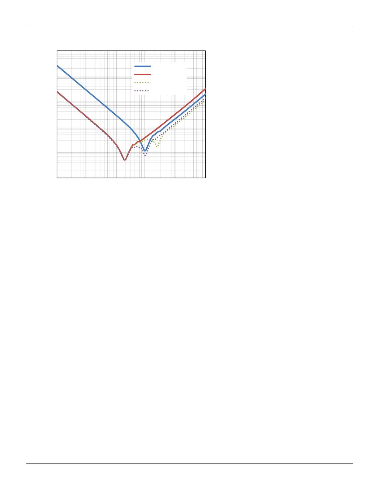
0.001
0.01
0.1
1
10
100
0.01 0.1 1 10 100 1000
Impedance (Ω)
Frequency (MHz)
1µF
10µF
10µF + 0.1µF
10µF + 0.47µF
Figure 2. Frequency characteristics of Ceramic capacitor
Figure 3-f shows unsuitable layout. Voltage noise will be
generated by the influence of wiring inductance for C
BYPASS
, V
IN
terminal and GND terminal of IC has some distance. Shortening
the wiring even by 1mm is highly recommended.
In case of buck converter, high frequency of several hundred
MHz will be loaded to the ground of C
IN
even with C
BYPASS
placed
close to IC. Therefore placing ground of C
IN
and C
O
must be
separated from each other by at least 1cm to 2cm.
Free-wheel diode D
1
must be placed closer and on same surface
of IC terminal. Figure 3-e shows suitable layout. With long
distance between IC terminal and diode, the spike noise will be
induced due to wiring inductance, that will be piled up at the
output. Use short and wide wiring for free-wheel diode, and
connect directly to GND terminal and switching terminal of IC.
Do not place it on bottom surface layer through via, as noise will
be worse, which is influenced by via inductance.
Figure 3-f shows unsuitable layout. Wiring inductance increases
due to distance between diode and switching terminal, and GND
terminal of IC and spike noise gets higher. To improve spike
noise caused by unsuitable layout the RC snubber-circuit may
be added as a countermeasure. This snubber-circuit must be
placed closer to switching terminal and GND terminal of IC
(Figure 3-g). Placing it at the both ends of diode will not absorb
spike noise generated by wiring inductance. (Figure 3-h).
Introduce Thermal Via
Copper area of PCB contributes to heat dissipation, but because
it does not have enough thickness, the heat dissipation result
that meets area cannot be achieved from limited PCB size. Heat
is dissipated using base material of board as a radiator. To
deliver heat to opposite layer of the board efficiently and to highly
reduce heat resistance, the thermal via are introduced.
Thermal via dimension of HTSOP-J8, reverse-side thermal pad
package is shown in Figure 4. To increase heat conductivity,
thermal via with small-diameter, inner diameter of 0.3mm which
can fill solder, is recommended. With large diameter, problem of
solder suction may occur at reflow solder process. Spacing
between thermal via is about 1.2mm and placed directly below
the thermal pad which is at the reverse-side of IC.
Place additional thermal via around IC like in Figure 3-a, if via
below the IC’s reverse-side thermal pad are not enough. Heat
sink of HTSOP-J8 reverse-side thermal pad package is at
ground potential, so EMI does not increase with wide copper
pattern.
C
IN
1µF 50V X5R GRM188R61H105KAAL (Murata)
10µF 50V X5R GRM31CR61H106KA12 (Murata)
C
BYPASS
0.1µF 50V X7R GRM188R71H104KA93 (Murata)
0.47µF 50V X7R GRM21BR71H474KA88 (Murata)
剩余11页未读,继续阅读
相关推荐


洁仔爱吃冰淇淋
- 粉丝: 4327
 我的内容管理
展开
我的内容管理
展开


最新资源
- WebDrive v16.00.4368: 简易易用的Windows风格FTP工具
- FirexKit:Python的FireX库组件
- Labview登录界面设计与主界面跳转实现指南
- ASP.NET JS引用管理器:解决重复问题
- HTML5 canvas绘图技术源代码下载
- 昆仑通态嵌入版ASD操舵仪软件应用解析
- JavaScript实现最小公倍数和最大公约数算法
- C++中实现XML操作类的方法与应用
- 设计编程工具集:材料重量快速计算指南
- Fancybox:Jquery图片轮播幻灯弹窗插件推荐
- Splunk Fitbit:全方位分析您的活动与睡眠数据
- Emoji表情编码资源及数据库查询实现
- JavaScript实现图片编辑:截取、旋转、缩放功能详解
- QNMS系统架构与应用实践
- 微软高薪面试题解析:通向世界500强的挑战
- 绿色全屏大气园林设计企业整站源码与多技术项目资源
