谷歌TPU架构解析:数据中心内的性能分析
下载需积分: 50 | PDF格式 | 3.24MB |
更新于2024-09-04
| 114 浏览量 | 举报
"这篇文档是关于Google的Tensor Processing Unit (TPU)的深入研究,它详细探讨了TPU的架构、性能以及各个组件的设计。文中还对比了TPU与传统GPU和CPU在数据中心内的表现,提供了全面的性能分析。作者团队由众多技术专家组成,涵盖了设计、工程和研究等多个领域,确保了研究的专业性和权威性。"
正文:
TPU(Tensor Processing Unit)是由Google设计的一种专门针对机器学习任务的加速硬件,特别是针对深度学习中的矩阵运算,如卷积神经网络(CNN)。这篇论文详尽阐述了TPU的架构及其优化策略,旨在提高计算效率和能效。
首先,TPU的核心设计理念是为了加速大规模机器学习模型的训练和推理过程。它被设计为一种高性能、低功耗的芯片,能够处理高度并行的计算任务,尤其适合在数据中心环境中运行。TPU的架构包含一个矩阵乘法单元(Matrix Multiply Unit,MMU),这个单元专为执行深度学习模型中的大规模矩阵运算而优化,这使得TPU在处理CNN等模型时速度远超传统的CPU和GPU。
其次,论文详细介绍了TPU的内存系统。TPU拥有高速的片上存储(On-chip Memory),可以快速访问频繁使用的数据,从而减少了对外部内存的依赖,降低了延迟,提高了整体性能。此外,TPU的内存架构还支持高效的并行数据读写,这对于深度学习模型的大规模训练至关重要。
再者,TPU的编程模型也是一大特色。它使用了专门的TensorFlow语言,可以直接对张量操作进行高效编译,减少了软件层面的开销。同时,TPU支持高效的模型并行和数据并行,允许用户在单个TPU或TPU集群上并行处理多个工作负载,进一步提升了计算效率。
论文还对比了TPU与GPU和CPU的性能。通常,GPU在图形渲染和通用计算方面表现出色,但其架构并不完全针对机器学习的特定需求。相比之下,TPU在机器学习任务上具有更高的计算密度和更低的延迟。CPU虽然通用性强,但在处理深度学习这样的密集计算任务时,往往效率较低。
Google的TPU是一种为深度学习定制的高性能计算硬件,通过优化的架构、内存系统和编程模型,实现了对大规模机器学习任务的高效加速。这篇论文为读者提供了深入理解TPU工作原理和性能优势的宝贵资料,对于研究人员和工程师来说,是探索硬件加速在深度学习领域应用的重要参考。
In-Datacenter Performance Analysis of a Tensor Processing Unit ISCA ’17, June 24-28, 2017, Toronto, ON, Canada
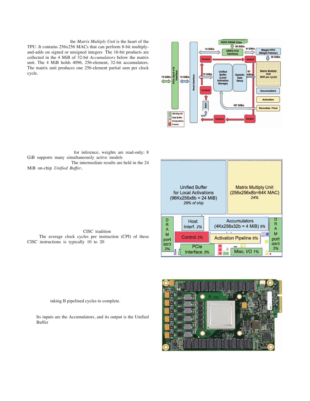
the upper-right corner, the Matrix Multiply Unit is the heart of the
TPU. It contains 256x256 MACs that can perform 8-bit multiply-
and-adds on signed or unsigned integers. The 16-bit products are
collected in the 4 MiB of 32-bit Accumulators below the matrix
unit. The 4 MiB holds 4096, 256-element, 32-bit accumulators.
The matrix unit produces one 256-element partial sum per clock
cycle. We picked 4096 by first noting that the operations per byte
needed to reach peak performance (roofline knee in Section 4) is
~1350, so we rounded that up to 2048 and then duplicated it so
that the compiler could use double buffering while running at
peak performance.
When using a mix of 8-bit weights and 16-bit activations (or
vice versa), the Matrix Unit computes at half-speed, and it
computes at a quarter-speed when both are 16 bits. It reads and
writes 256 values per clock cycle and can perform either a matrix
multiply or a convolution. The matrix unit holds one 64 KiB tile
of weights plus one for double buffering (to hide the 256 cycles it
takes to shift a tile in). This unit is designed for dense matrices.
Sparse architectural support was omitted for time-to-deployment
reasons. The weights for the matrix unit are staged through an on-
chip Weight FIFO that reads from an off-chip 8 GiB DRAM
called Weight Memory (for inference, weights are read-only; 8
GiB supports many simultaneously active models). The weight
FIFO is four tiles deep. The intermediate results are held in the 24
MiB on-chip Unified Buffer, which can serve as inputs to the
Matrix Unit. A programmable DMA controller transfers data to or
from CPU Host memory and the Unified Buffer.
Figure 2 shows the floor plan of the TPU die. The 24 MiB
Unified Buffer is almost a third of the die and the Matrix Multiply
Unit is a quarter, so the datapath is nearly two-thirds of the die.
The 24 MiB size was picked in part to match the pitch of the
Matrix Unit on the die and, given the short development schedule,
in part to simplify the compiler (see Section 7). Control is just 2%.
Figure 3 shows the TPU on its printed circuit card, which inserts
into existing servers like an SATA disk.
As instructions are sent over the relatively slow PCIe bus,
TPU instructions follow the CISC tradition, including a repeat
field. The average clock cycles per instruction (CPI) of these
CISC instructions is typically 10 to 20. It has about a dozen
instructions overall, but these five are the key ones:
1. Read_Host_Memory reads data from the CPU host
memory into the Unified Buffer (UB).
2. Read_Weights reads weights from Weight Memory
into the Weight FIFO as input to the Matrix Unit.
3. MatrixMultiply/Convolve causes the Matrix
Unit to perform a matrix multiply or a convolution from the
Unified Buffer into the Accumulators. A matrix operation
takes a variable-sized B*256 input, multiplies it by
a
256x256 constant weight input, and produces a B*256
output, taking B pipelined cycles to complete.
4. Activate
performs the nonlinear function of the
artificial neuron, with options for ReLU, Sigmoid, and so on.
Its inputs are the Accumulators, and its output is the Unified
Buffer. It can also perform the pooling operations needed for
convolutions using the dedicated hardware on the die, as it i
s
connected to nonlinear function logic.
5. Write_Host_Memory writes data from the Unified
Buffer into the CPU host memory.
The other instructions are alternate host memory read/write, set
configuration, two versions of synchronization, interrupt host,
Figure 1. TPU Block Diagram. The main computation is the
yellow Matrix Multiply unit. Its inputs are the blue Weight
FIFO and the blue Unified Buffer and its output is the blue
Accumulators. The yellow Activation Unit performs the
nonlinear functions on the Accumulators, which go to the
Unified Buffer.
Figure 2. Floorplan of TPU die. The shading follows Figure 1.
The light (blue) datapath is 67%, the medium (green) I/O is
10%, and the dark (red) control is just 2% of the die. Control
is much larger (and much harder to design) in a CPU or GPU.
Figure 3. TPU Printed Circuit Board. It can be inserted into
the slot for a SATA disk in a server.
3
剩余11页未读,继续阅读
相关推荐


jingjiniaooo
- 粉丝: 1
 我的内容管理
展开
我的内容管理
展开


最新资源
- UMLChina:系统建模与设计关键要素详解
- Prototype中文API详解与实用函数
- 复杂网络结构与功能研究综述
- 电脑判案与法律推理:人工智能在司法中的角色探讨
- 《深入浅出MFC》2/e电子书免费下载
- 使用C#操作Excel:从入门到精通
- 正则表达式基础与高级技巧详解
- C#设计模式手册:单例、工厂到访问者模式解析
- Eclipse插件开发实战:从安装到SWTDesigner应用
- Visual Studio .NET使用技巧全览:2004-2007精华
- Ant入门教程:构建Java项目的必备指南
- Log4j配置与使用详解
- 探索Eclipse:使用指南与插件开发详解
- 网页开发:200个常用JSP脚本与JavaScript技巧
- 深入解析bash-door后门机制
- 快速排序算法详解与实现
