Wideband Vertically-Interdigital-Capacitor
Bo Zhou, Lingxuan Huang, Qipeng Chen, Xuan Ni, Xiuxian Li, Ninglin Wang, Zhikuang Cai*
Nanjing University of Posts and Telecommunications
#9, Wenyuan Road
Nanjing City 210003,
People’s Republic of China
Phone 0086-13851735758 and E-mail: sarahxboy@hotmail.com
Abstract
Abstract—A wideband vertically-interdigital-capacitor
(WBVIC) is proposed in a 10-layer low temperature co-fired
ceramic (LTCC) substrate. By interconnecting the open ends of
interval fingers with vertical via interconnections outside the
vertically-interdigital-capacitor (VIC), the spurious spikes that
limit the bandwidth of VIC are suppressed. The bandwidth and
capacitance of VIC increased 100% and 20%, respectively.
Keywords—Wideband;vertically-interdigital-capacitor(VIC),
spurious spikes suppression.
I
INTRODUCTION
Vertically-interdigital-capacitor (VIC) is usually used
to build lumped filters or couplers in multi-layered
substrates because of its large capacitance, higher
Q-value and small size [1-8]. The structure of
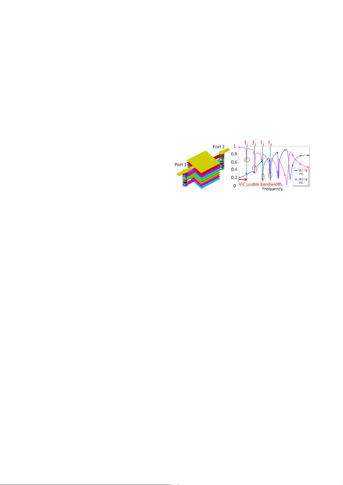
conventional VIC is shown in Fig. 1(a). Normally the
lower application frequency, the higher capacitance is
required. Capacitance increment of VIC can be reached
if the size or the number of fingers is increased. However,
increasing the size of fingers is in conflict with size
reduction. And increasing the number of fingers results
in unwanted resonances at frequencies f
1
, f
2
, f
3
and f
4
,
which limits its working band, shown in Fig. 1(b).
Because VIC is a multi-finger structure, which presents
multi-conductor configuration and shows multiple pass
bands and stop bands in its equivalent circuit. All VICs
have this problem when designed and built. Bond wire
was proposed to eliminate the spikes of planar style
interdigital capacitors in [9-10], but it’s not available for
VIC as its fingers are buried into the multi-layered
substrate. Via transitions and ground clearances inside
VIC is proposed to suppress the unwanted spurious
spikes [11], but the structure inside VIC is quite complex,
which is not good for fabrication with a satisfied product
yield. Moreover, if the pad of VIC is too small, it is
impossible to embed via transitions inside VIC. So the
structure using inside via transitions and clearances [5]
have limitations when designed.
In this paper, a wideband
vertically-interdigital-capacitor (WBVIC) is proposed in
a 10-layer low temperature co-fired ceramic (LTCC)
substrate. With short interconnecting the open ends of
interval fingers using vertical via interconnections
outside VIC structure, spurious spikes suppression and
capacitance increment are both achieved. The bandwidth
and capacitance of VIC increased 100% and 20%,
respectively.
(a) (b)
Fig.1 Conventional VIC with 8 fingers (a) structure and (b) corresponding
S-parameters.
II
CIRCUIT IMPLEMENTATION
The WBVIC with eight square fingers is proposed with
vertical via interconnections. The open ends of interval
fingers are interconnected using via transitions, which
are used to suppress the unexpected spurious spikes.
View from Port 1, Fingers 2, 4, 6 and 8 are
interconnected with vertical via interconnections outside
VIC, shown in Fig. 2(a). And view from Port 2, Fingers 1,
3, 5 and 7 are interconnected with vertical via
interconnections outside VIC, shown in Fig. 2(b). In Fig.
3(a), a finger is equivalent to a series inductance and
capacitive coupling between adjacent fingers is marked
by the capacitances Cij, where i and j are the finger
numbers. Fig. 3(b) shows how the equivalent circuit is
changed when the vertical via interconnections are
installed. Therefore, the unwanted spikes in the
frequency response are removed as the number of stop
bands is decreased. Fig.3 also illustrates capacitance
increment with regrouping the equivalent inductances
and capacitances.
The proposed WBVIC is fabricated in a 10-layer
Ferro-A6 LTCC substrate. Each layer has a post-fired
thickness of 0.1 mm with a dielectric constant of 5.9 and
loss tangent of 0.002. The EM-simulation is using
AXIEM, which is a full-wave electromagnetic (EM)
simulator [12]. The final optimal parameters are: W
1
=0.3
mm, W
2
=0.2 mm, W
3
=0.4 mm and W
C
=1.6 mm, where
the parameters are defined in Fig. 4(a). The photograph
978-1-5386-5442-2/18/$31.00 ©2018 IEEE
201


