"TI LVDS缓冲器SN65LVP19.pdf详解及特性"
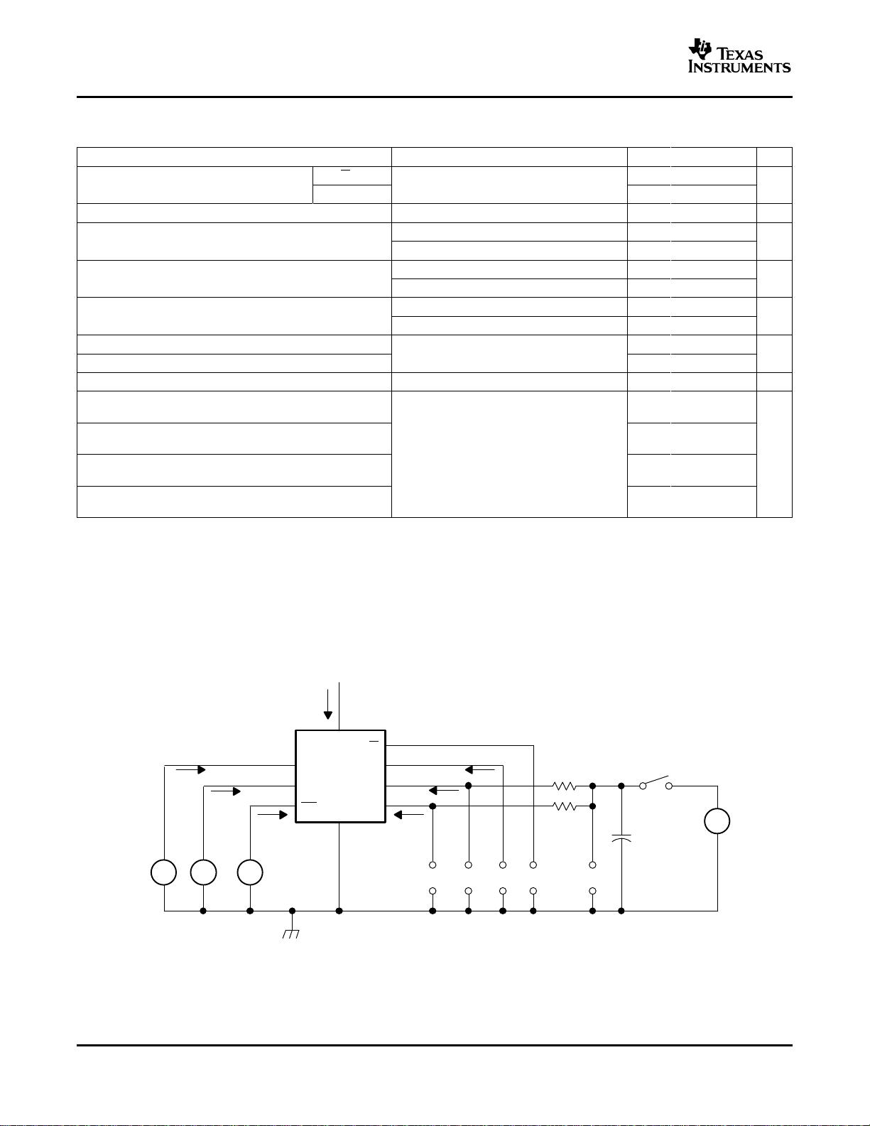
The TI-SN65LVP19.pdf is a document that describes LVDS buffer devices, specifically the SN65LVDS18 and SN65LVP18, as well as the SN65LVDS19 and SN65LVP19. These devices have a VCC voltage of 2.5V or 3.3V and feature a 4mA VREF. They come in a 2mm x 2mm small-outline no-lead package, making them suitable for a variety of applications.
The LVDS buffer devices are designed for use in oscillator gain stage and buffer applications. They have low-voltage PECL inputs and low-voltage PECL or LVDS outputs, with clock rates up to 1 GHz. The devices can perform PECL-to-LVDS translation with 250ps output transition times, as well as clock signal amplification with 0.12ps typical intrinsic phase jitter.
Overall, the LVDS buffer devices from TI offer high performance and reliability for a range of applications requiring precise and stable clock signals. Their compact size, low power consumption, and fast transition times make them an ideal choice for design engineers looking for quality LVDS buffer devices.
2023-02-08 上传
2023-02-08 上传
154 浏览量
2023-07-26 上传
2020-05-30 上传
2021-04-08 上传
点击了解资源详情
点击了解资源详情
不觉明了
- 粉丝: 4788
- 资源: 5759
最新资源
- Angular实现MarcHayek简历展示应用教程
- Crossbow Spot最新更新 - 获取Chrome扩展新闻
- 量子管道网络优化与Python实现
- Debian系统中APT缓存维护工具的使用方法与实践
- Python模块AccessControl的Windows64位安装文件介绍
- 掌握最新*** Fisher资讯,使用Google Chrome扩展
- Ember应用程序开发流程与环境配置指南
- EZPCOpenSDK_v5.1.2_build***版本更新详情
- Postcode-Finder:利用JavaScript和Google Geocode API实现
- AWS商业交易监控器:航线行为分析与营销策略制定
- AccessControl-4.0b6压缩包详细使用教程
- Python编程实践与技巧汇总
- 使用Sikuli和Python打造颜色求解器项目
- .Net基础视频教程:掌握GDI绘图技术
- 深入理解数据结构与JavaScript实践项目
- 双子座在线裁判系统:提高编程竞赛效率


