16nm FinFET工艺在28Gb/s SerDes模拟前端设计中的挑战与解决方案
"这篇论文由Avago Technologies的工程师Freeman Zhong和Ashutosh Sinha在2014年撰写,探讨了在16nm FinFET半导体工艺中设计高速SerDes(串行器/解串器)模拟前端的问题。论文主要关注28Gb/s SerDes,比较了28nm平面CMOS工艺与16nm FinFET工艺对电路性能的影响,并提出了一些应对技术来减轻不良设备特性的影响。"
在高速通信系统中,SerDes扮演着至关重要的角色。随着数据流量的指数级增长和半导体工艺的进步,SerDes的数据速率已从1.25Gb/s提升至28+Gb/s。一个典型的串行链路包括发射机、信道和接收机,它不仅负责数据的串行化(N到1位)和反串行化(1到N位),还包含了通道均衡等功能,以确保在高速传输下的信号完整性。
传统的28nm平面CMOS工艺在制造高速SerDes时面临一些挑战,如信号衰减、噪声和功耗问题。而16nm FinFET工艺引入了三维鳍式场效应晶体管,其更小的尺寸和更好的栅极控制理论上能提供更高的速度、更低的功耗以及更好的性能。然而,FinFET工艺也带来了新的设计难题,如寄生效应、工艺变异性以及热效应等。
论文中详细讨论了几种架构选择,以及在16nm FinFET工艺下如何设计模拟电路来应对这些挑战。这可能包括优化的电路拓扑结构,如差分放大器、均衡器和时钟恢复电路的改进设计。为了减轻FinFET工艺特有的不良设备特性,论文提出了各种技术和策略,例如使用补偿电路来减少噪声,采用新型的电源管理方案来降低功耗,以及采用先进的信号处理算法来改善信道性能。
通过应用这些先进技术及缓解措施,作者开发出了一款原型28Gb/s SerDes,并展示了理想的性能、功耗和芯片面积。实验结果证明,16nm FinFET工艺在实现高速SerDes方面具有显著优势,但同时也强调了在设计过程中对模拟电路和设备特性的深入理解是至关重要的。
"Analog Circuit and Device Interaction in High-Speed SerDes"论文提供了对高速SerDes设计的深入洞察,尤其是在16nm FinFET工艺中的挑战和解决方案,对于理解和优化这类高速通信组件具有重要价值。
Analog Circuit and Device Interaction in High-Speed SerDes Design in 16nm
FinFET CMOS Technology
Freeman Zhong, Ashutosh Sinha
Avago Technologies Inc, San Jose, CA 95131
Abstract
SerDes deals with data serialization, deserialization and
channel equalization up to data rate of 28+Gb/s. Process
technology and device characteristic greatly impacts
architecture, circuit topology, and design merit of a SerDes.
Several architecture choices, analog circuits, and techniques
to mitigate undesired device characteristic in 16nm FinFET
are discussed in this paper. With advanced CMOS technology
and mitigation techniques, a prototype 28Gb/s SerDes was
developed and demonstrated desired performance, power and
die area.
Introduction
SerDes is one of the most critical components in
communication systems. As data traffic increases
exponentially and CMOS technology advances to 16nm in
past 15 years, data rate of SerDes has increased from
1.25Gb/s to 28+Gb/s. As shown in Fig. 1, 2, 3, a serial link
consists of a transmitter, channel, and receiver. It not only
functions as data serialization from N to 1 bit, and
deserialization from 1 to N bit, but also deals with signal
integrity challenges, such as inter-symbol-interference, cross-
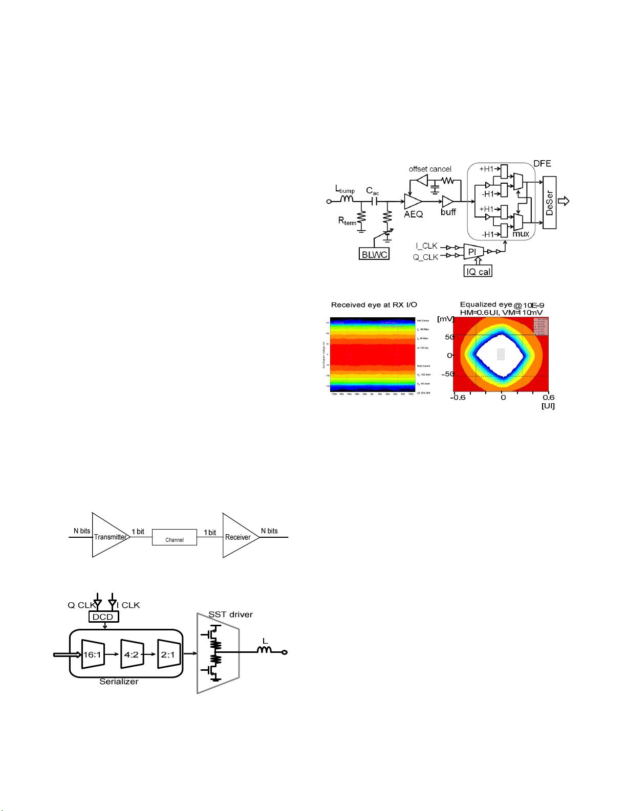
talk, reflection and system jitter as data rate increases. Due to
low-pass nature of a channel, the received eye is totally
closed at a receiver. With channel equalization from both
transmitter and receiver, the equalized eye is open enough for
clock and data recovery as shown in Fig. 4. Many SerDes
were designed and fabricated in 250nm to 28nm CMOS
technology (1), (2), (3).
Fig. 1– Block diagram of a serial link
Fig. 2 – Block diagram of a transmitter
Figure 3 – Block diagram of a receiver
Fig. 4 – Received and equalized eyes at a receiver with 28Gb/s PRBS31 data
traffic over a channel of 34dB loss
SerDes architecture and process technology interaction
Process technology greatly impacts the architecture,
implementation, performance and power consumption of a
SerDes. The critical process parameters, such as unity gain
frequency, threshold voltage, leakage, and maximum supply
voltage of devices, are dominant considerations for SerDes
architecture choice. For example, a decision feedback
equalizer (DFE) is a timing critical circuit that generates a
feedback signal and adds it to the received signal within one
unit interval (UI). For data rate below 16Gb/s, direct
feedback DFE, as shown in Fig. 5, is an optimal
implementation where the timing constraint of Tck-q + Tdac
+ Tsum + Tsetup < 1UI can be met in in 28nm/16nm process.
However, when data rate increases to 28Gb/s where 1UI is
only 35.7ps, the timing constraint of direct DFE is no longer
met. A h1 loop unrolled DFE, shown in Fig. 6, was
developed where the +/-h1 feedback signals are pre-
calculated and added to received signal, and 2 speculative
outputs are selected based on previous data decision, thus,
new timing constraint of Tck-q + Tmux + Tsetup < 1UI can
be met in 28nm/16nm CMOS.
As CMOS technology scales down to16nm, thin-oxide device
operates at lower supply voltage that presents challenges of
headroom and linearity to analog circuits. To tackle these
3.2.1 IEDM14-52978-1-4799-8001-7/14/$31.00 ©2014 IEEE
下载后可阅读完整内容,剩余3页未读,立即下载
2020-11-29 上传
2019-09-07 上传
2023-02-10 上传
2024-05-28 上传
2023-05-26 上传
2023-05-19 上传
2023-03-28 上传
2023-05-21 上传

whyyfdr
- 粉丝: 7
- 资源: 9
 我的内容管理
展开
我的内容管理
展开


最新资源
- 磁性吸附笔筒设计创新,行业文档精选
- Java Swing实现的俄罗斯方块游戏代码分享
- 骨折生长的二维与三维模型比较分析
- 水彩花卉与羽毛无缝背景矢量素材
- 设计一种高效的袋料分离装置
- 探索4.20图包.zip的奥秘
- RabbitMQ 3.7.x延时消息交换插件安装与操作指南
- 解决NLTK下载停用词失败的问题
- 多系统平台的并行处理技术研究
- Jekyll项目实战:网页设计作业的入门练习
- discord.js v13按钮分页包实现教程与应用
- SpringBoot与Uniapp结合开发短视频APP实战教程
- Tensorflow学习笔记深度解析:人工智能实践指南
- 无服务器部署管理器:防止错误部署AWS帐户
- 医疗图标矢量素材合集:扁平风格16图标(PNG/EPS/PSD)
- 人工智能基础课程汇报PPT模板下载
