MPEG音频编码器中改进的MDCT算法
"MPEG音频编码器中的MDCT算法优化"
MPEG音频编码器中的多分辨率离散余弦变换(MDCT)是音频压缩技术的核心组件,用于高效地处理音频信号。MDCT是一种线性变换,它能够将时域信号转换为频域表示,从而在保持音质的同时,有效地减少数据量,适合于音频编码和存储。
在"Improved Algorithm for Efficient Computation of the Forward and Backward MDCT in MPEG Audio Coder"中,作者探讨了提高MDCT计算效率的方法。MDCT的前向和后向变换是MPEG音频编码过程的关键步骤,它们涉及到大量的计算操作,包括加法、乘法和取模运算。为了优化这些计算,研究者通常寻找减少硬件资源需求的策略,如ROM空间的利用。
文章提到,作者试图利用特定的性质来减少ROM的空间需求,特别是对于模2p+2的地址,期望通过减少2位来节省ROM空间。然而,他们发现仅依赖2p+2的标度残差无法提供足够的信息(如符号和对称性)来实现这种ROM需求的降低。这意味着,尽管可以尝试通过残差的最高两位来简化处理,但这种方法并不总是有效。
为了进一步优化相位累加器的延迟,Chren建议使用有限状态机(FSM)代替基于二进制加法器和2:1多路复用器的模加器。FSM的使用可以将延迟减少到只有两个逻辑级别,这对于实时处理是至关重要的。此外,通过在中国剩余定理(CRT)上处理残差,可以直接获取供数模转换器(DAC)使用的采样值。图1(b)中的地址反向(AI)块执行模逆运算,以实现对称性的功能。
Chren还在参考文献[1]和[2]中提出了另一种架构设计,该设计减少了面积需求,可能包括更紧凑的数据结构和计算流程。这种架构优化不仅有助于提高计算速度,还能降低硬件实现的成本,是MPEG音频编码器设计中的一个重要进步。
MDCT在MPEG音频编码中的优化是一个持续的研究领域,旨在平衡计算效率、资源利用率和音频质量。本文提供的改进算法和设计思路对于理解和改进现代音频编解码器的内部工作原理具有重要价值。
990 IEEE TRANSACTIONS ON CIRCUITS AND SYSTEMS—II: ANALOG AND DIGITAL SIGNAL PROCESSING, VOL. 48, NO. 10, OCTOBER 2001
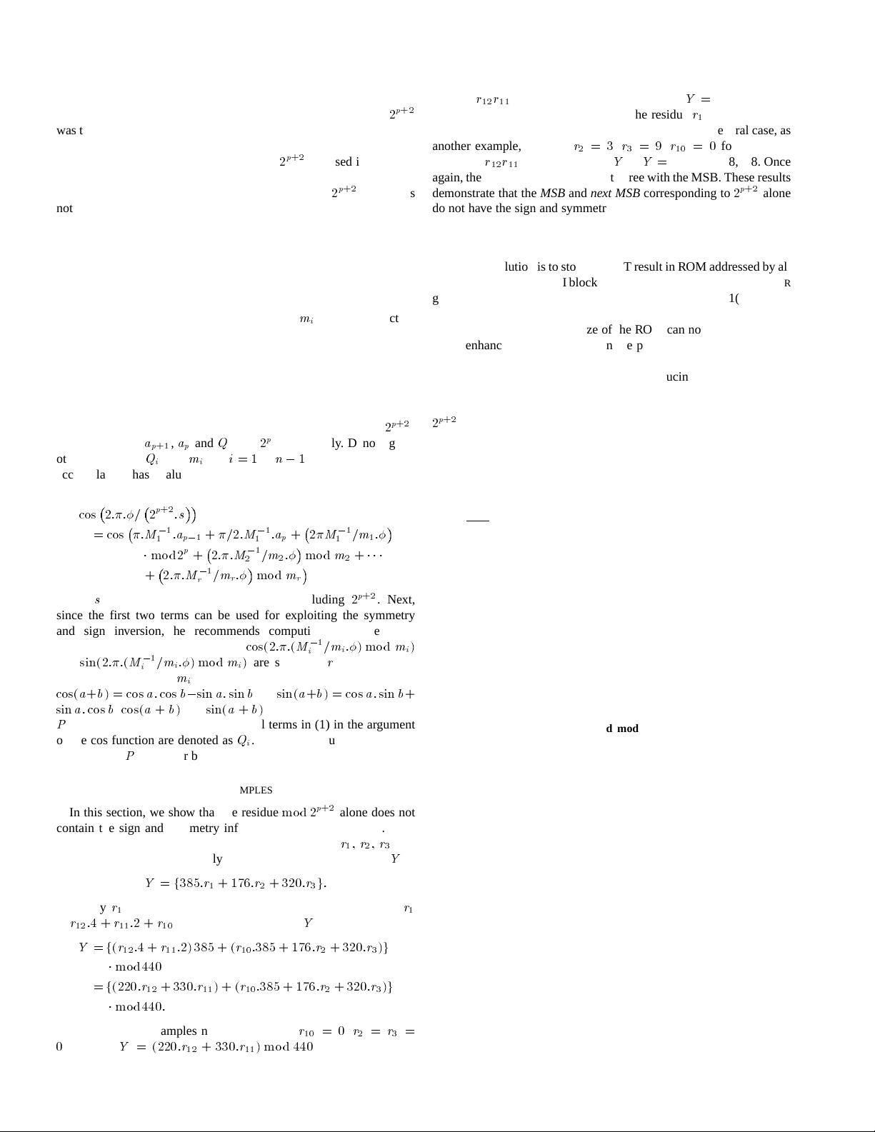
the ROM space as mentioned before. The author used the same prop-
erty for the RNS form also. Thus, the ROM address for moduli
2
p
+2
was thought to be made less by 2 bits saving ROM space for this mod-
ulus. While residues of all the moduli directly address the ROM, the
two MSBs of the residue corresponding to
2
p
+2
are used in the same
manner as in the case of the other residues. Unfortunately, we show by
example in the next section, that the scaled residue of
2
p
+2
alone does
not contain the sign and symmetry information to facilitate such reduc-
tion in ROM requirements.
Chren recommends the use of a finite state machine (FSM) in place
of modulo adder (using binary adders and 2: 1 multiplexers as de-
scribed earlier) for the phase accumulator, since the delay can be of
only two logic levels. The samples to be fed to the DAC can be ob-
tained by using CRT on the residues. The address invert (AI) block in
Fig. 1(b), performs the additive inverse modulo
m
i
so that the function
of symmetry can be achieved.
Chren [1], [2] suggests another architecture reduced area direct
synthesizer (RADS) for reducing the area. Herein, the sample values
are computed rather than stored. The block diagram is as shown in
Fig. 1(c). Here, the phase accumulator used adders because they can be
smaller. We first note that in both the schemes of Fig. 1(b) and (c), the
two MSBs and the remaining LSB word in the first residue (i.e.,
2
p
+2
)
were denoted as
a
p
+1
,
a
p
and
Q
mod
2
p
, respectively. Denoting the
other residues as
Q
i
mod
m
i
, for
i
=1
to
n
0
1
, Chren computes the
accumulated phase value using Chinese Remainder Theorem (CRT)
for generating every output sample
cos 2
::=
2
p
+2
:
s
= cos
:
M
0
1
1
:
a
p
0
1
+
=
2
:
M
0
1
1
:
a
p
+ 2
M
0
1
1
=
m
1
:
1
mod2
p
+ 2
::
M
0
1
2
=
m
2
:
mod
m
2
+
111
+
2
::
M
0
1
r
=
m
r
:
mod
m
r
(1)
where
s
is the product of all the moduli excluding
2
p
+2
. Next,
since the first two terms can be used for exploiting the symmetry
and sign inversion, he recommends computing only the other
terms. Hence, considering that
cos(2
::
(
M
0
1
i
=
m
i
:
)mod
m
i
)
and
sin(2
::
(
M
0
1
i
=
m
i
:
)mod
m
i
)
are stored in
r
locations each
corresponding to each
m
i
, using the basic cosine and sine identities
cos(
a
+
b
) = cos
a
:
cos
b
0
sin
a
:
sin
b
and
sin(
a
+
b
) = cos
a
:
sin
b
+
sin
a
:
cos
b
,
cos(
a
+
b
)
and
sin(
a
+
b
)
are computed by a processor
P
as described in Fig. 1. The individual terms in (1) in the argument
of the cos function are denoted as
Q
i
. The scaler is used to scale the
output of the
P
processor by the product of the overflow moduli.
II. E
XAMPLES
In this section, we show that the residue
mod 2
p
+2
alone does not
contain the sign and symmetry information through examples. Con-
sider the moduli set {8,5,11}. Denoting the residues as
r
1
;
r
2
;
r
3
cor-
responding to these, respectively, the use of CRT yields the result
Y
as
Y
=
f
385
:
r
1
+ 176
:
r
2
+320
:
r
3
g
:
Evidently,
r
1
is a 3-bit word corresponding to residue of 8. Writing
r
1
as
r
12
:
4+
r
11
:
2+
r
10
, Chren suggests writing
Y
as
Y
=
f
(
r
12
:
4+
r
11
:
2) 385 + (
r
10
:
385 + 176
:
r
2
+ 320
:
r
3
)
g
1
mod440
=
f
(220
:
r
12
+ 330
:
r
11
)+(
r
10
:
385 + 176
:
r
2
+ 320
:
r
3
)
g
1
mod440
:
We consider two examples next. For the case
r
10
=0
,
r
2
=
r
3
=
0
,wehave
Y
= (220
:
r
12
+ 330
:
r
11
) mod 440
giving for the four
cases of
r
12
r
11
viz., 00,01,10, and 11 the results
Y
=
0,330,220, and
110. Thus, the MSB and next MSB of the residue
r
1
do not correctly
determine the sign and symmetry information. For the general case, as
another example, consider
r
2
=3
,
r
3
=9
,
r
10
=0
for which we
obtain for
r
12
r
11
viz., 00,01,10,11
Y
as
Y
=
328,218,108,438. Once
again, the sign of the result does not agree with the MSB. These results
demonstrate that the MSB and next MSB corresponding to
2
p
+2
alone
do not have the sign and symmetry information.
III. C
ONCLUSION
The only solution is to store the CRT result in ROM addressed by all
the residues. Hence, the AI blocks, the MSB, and nextMSB exclusive
OR
gate and sign inversion blocks in Chren architecture in Fig. 1(b) are also
not useful due to the direct nonavailability of symmetry information.
It is evident, hence, that the size of the ROM can not be reduced. The
speed enhancement is thus only in the phase accumulator which can
be of smaller word length, while scaling actually introduces additional
operations decreasing the speed, however, reducing the memory space
needed. Note that in the case of low area version also, the same obser-
vations apply. However, note that the ROM corresponding to residue of
2
p
+2
uses all the bits as address. The AI blocks and exclusive
OR gate
for MSB and next MSB are also not required.
R
EFERENCES
[1] W. A. Chren, Jr., “RNS-base enhancements for direct digital frequency
synthesis,” IEEE Trans. Circuits Syst. II, vol. 42, pp. 516–524, 1995.
[2]
, “One-hot residue coding for low-delay power product CMOS de-
sign,” IEEE Trans. Circuits Syst. II, vol. 45, pp. 303–313, 1998.
Improved Algorithm for Efficient Computation of the
Forward and Backward MDCT in MPEG Audio Coder
Szu-Wei Lee
Abstract—Britanak recently proposed an efficient algorithm to im-
plement the forward and backward modified discrete cosine transform
(MDCT) in MPEG layer III [9]. Britanak’s algorithm employs discrete
cosine transform of type II (DCT-II) and discrete sine transform of type
II (DST-II) to compute the forward MDCT, and uses their inverses to
compute the backward MDCT. This brief presents an improved algorithm
to implement the forward and backward MDCT in MPEG layer III.
Notably, the proposed algorithm requires less calculation than Britanak’s
algorithm does. Furthermore, it employs the same module to compute both
the forward and backward MDCT. Thus, when compared to Britanak’s
algorithm, the proposed algorithm is implemented more easily.
Index Terms—Audio coding, modified discrete cosine transform
(MDCT), MPEG.
I. INTRODUCTION
The time domain aliasing cancelation (TDAC) filter bank is a good
tool to analyze and synthesize signals [1], and it has been employed
Manuscript received February 2, 2001; revised September 20, 2001. This
paper was recommended by Associate Editor A. Skodros.
The author is with Intervideo Int. Inc., Taichung, Taiwan, R.O.C. (e-mail:
swli@ms14.hinet.net).
Publisher Item Identifier S 1057-7130(01)11055-4.
1057–7130/01$10.00 © 2001 IEEE
Authorized licensed use limited to: IEEE Xplore. Downloaded on March 11, 2009 at 05:53 from IEEE Xplore. Restrictions apply.
下载后可阅读完整内容,剩余4页未读,立即下载
335 浏览量
2022-09-24 上传
点击了解资源详情
2022-09-24 上传
2022-09-20 上传
2022-09-24 上传
153 浏览量
2022-09-21 上传
2022-09-20 上传

GnuMake
- 粉丝: 0
 我的内容管理
展开
我的内容管理
展开


最新资源
- 网狐工具:核心DLL和程序文件解析
- PortfolioCVphp - 展示JavaScript技能的个人作品集
- 手机归属地查询网站完整项目:HTML+PHP源码及数据集
- 昆仑通态MCGS通用版S7400父设备驱动包下载
- 手机QQ登录工具的压缩包内容解析
- Git基础学习仓库:掌握版本控制要点
- 3322动态域名更新器使用教程与下载
- iOS源码开发:温度转换应用简易教程
- 定制化用户登录页面模板设计指南
- SMAC电机在包装生产线应用的技术案例分析
- Silverlight 5实现COM组件调用无需OOB技术
- C#实现多功能画图板:画直线、矩形、圆等
- 深入探讨C#语言在WPF项目开发中的应用
- 新版2012109通用权限系统源码发布:多角色用户支持
- 计算机科学与工程系网站开发技术源码合集
- Java实现简易导出Excel工具的开发教程
