18 INTRODUCTION Chapter 1
profound effect on these global signals. For instance, connecting more cells to a sup-
ply line can cause a voltage drop over the wire, which, in its turn, can slow down all
the connected cells. Issues such as clock distribution, circuit synchronization, and
supply-voltage distribution are becoming more and more critical. Coping with them
requires a profound understanding of the intricacies of digital circuit design.
• Another impact of technology evolution is that new design issues and constraints
tend to emerge over time. A typical example of this is the periodical reemergence of
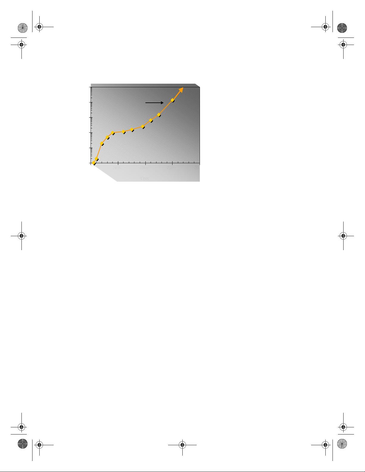
power dissipation as a constraining factor, as was already illustrated in the historical
overview. Another example is the changing ratio between device and interconnect
parasitics. To cope with these unforeseen factors, one must at least be able to model
and analyze their impact, requiring once again a profound insight into circuit topol-
ogy and behavior.
• Finally, when things can go wrong, they do. A fabricated circuit does not always
exhibit the exact waveforms one might expect from advance simulations. Deviations
can be caused by variations in the fabrication process parameters, or by the induc-
tance of the package, or by a badly modeled clock signal. Troubleshooting a design
requires circuit expertise.
For all the above reasons, it is my belief that an in-depth knowledge of digital circuit
design techniques and approaches is an essential asset for a digital-system designer. Even
though she might not have to deal with the details of the circuit on a daily basis, the under-
standing will help her to cope with unexpected circumstances and to determine the domi-
nant effects when analyzing a design.
Example 1.1 Clocks Defy Hierarchy
To illustrate some of the issues raised above, let us examine the impact of deficiencies in one
of the most important global signals in a design, the clock. The function of the clock signal in
a digital design is to order the multitude of events happening in the circuit. This task can be
compared to the function of a traffic light that determines which cars are allowed to move. It
also makes sure that all operations are completed before the next one starts—a traffic light
should be green long enough to allow a car or a pedestrian to cross the road. Under ideal cir-
cumstances, the clock signal is a periodic step waveform with transitions synchronized
throughout the designed circuit (Figure 1.7a). In light of our analogy, changes in the traffic
lights should be synchronized to maximize throughput while avoiding accidents. The impor-
tance of the clock alignment concept is illustrated with the example of two cascaded registers,
both operating on the rising edge of the clock φ (Figure 1.7b). Under normal operating condi-
tions, the input In gets sampled into the first register on the rising edge of φ and appears at the
output exactly one clock period later. This is confirmed by the simulations shown in Figure
1.8c (signal Out).
Due to delays associated with routing the clock wires, it may happen that the clocks
become misaligned with respect to each other. As a result, the registers are interpreting time
indicated by the clock signal differently. Consider the case that the clock signal for the second
register is delayed—or skewed—by a value δ. The rising edge of the delayed clock φ′ will
postpone the sampling of the input of the second register. If the time it takes to propagate the
output of the first register to the input of the second is smaller than the clock delay, the latter
will sample the wrong value. This causes the output to change prematurely, as clearly illus-
trated in the simulation, where the signal Out′ goes high at the first rising edge of φ′ instead of
chapter1.fm Page 18 Friday, January 18, 2002 8:58 AM


