
Input Voltage (V)
Output Voltage (V)
3.25 3.5 3.75 4 4.25 4.5 4.75 5 5.25 5.5
-3.375
-3.35
-3.325
-3.3
-3.275
-3.25
-3.225
-3.2
-3.175
-3.15
-3.125
-3.1
D017
0 mA
50 mA
100 mA
Input Voltage (V)
Output Voltage (V)
3.25 3.5 3.75 4 4.25 4.5 4.75 5 5.25 5.5
3.275
3.28
3.285
3.29
3.295
3.3
3.305
3.31
D018
0 mA
50 mA
100 mA
Output Current (mA)
Dropout Voltage (mV)
0 25 50 75 100 125 150 175 200 225 250
0
20
40
60
80
100
120
D015
VOUT+
VOUT-
I
OUT
(A)
R
CP
(:)
0.001 0.01 0.1 0.5
1
10
100
500
D016
85°C
25°C
-40°C
Output Current (mA)
Output Voltage Ripple (mV)
0 25 50 75 100 125 150 175 200 225 250
0.5
1
1.5
2
2.5
3
3.5
4
4.5
5
D014
VOUT+
VOUT-
Input Voltage (V)
Output Voltage Ripple (mV)
2.8 3 3.2 3.4 3.6 3.8 4 4.2
1
1.2
1.4
1.6
1.8
2
2.2
2.4
2.6
2.8
3
D022
VOUT-
VOUT+
6
LM27762
ZHCSFJ0B –AUGUST 2016–REVISED FEBRUARY 2017
www.ti.com.cn
版权 © 2016–2017, Texas Instruments Incorporated
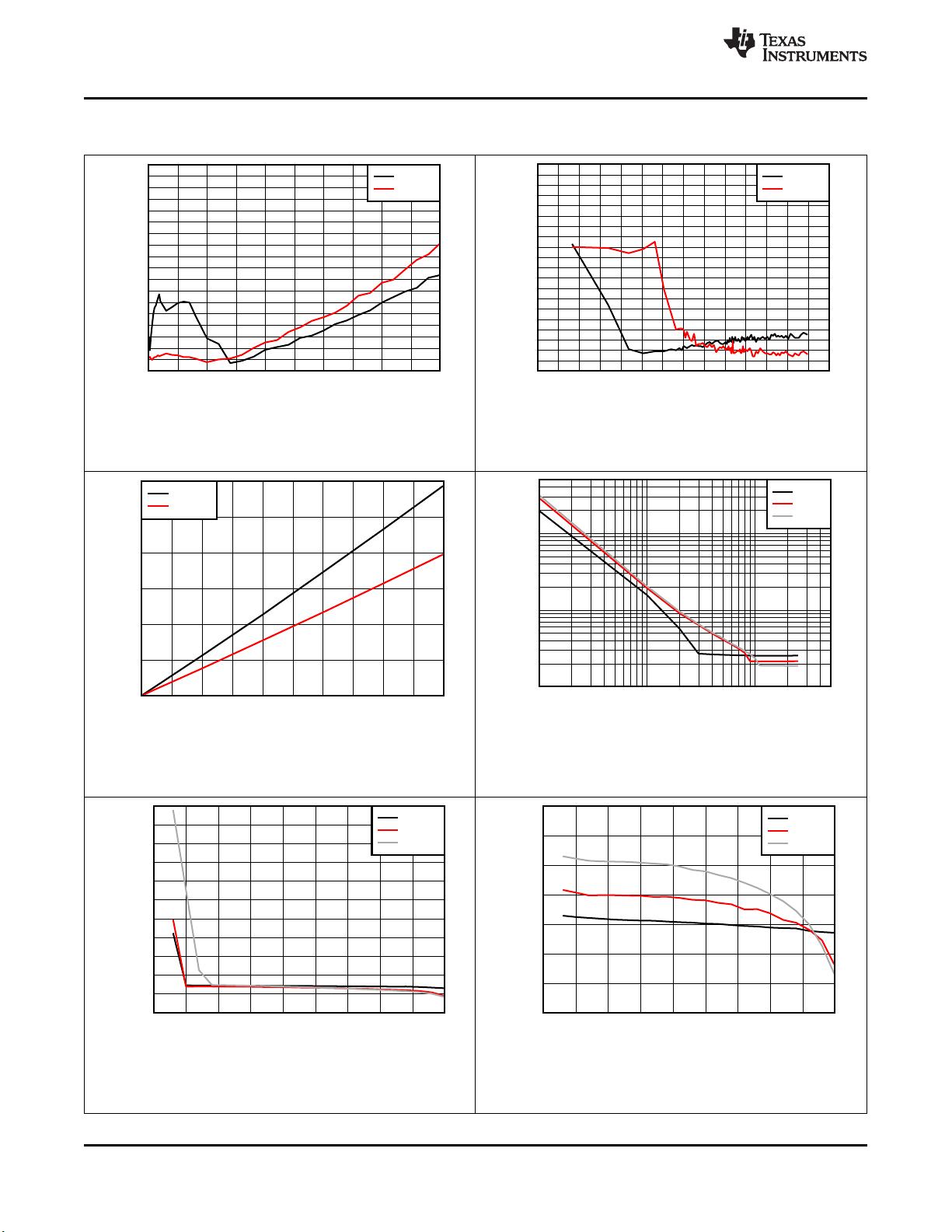
6.6 Typical Characteristics
V
IN
= 3.7 V V
OUT
= ± 3 V
图图 1. Output Voltage Ripple vs Output Current
V
OUT
= ± 3 V I
OUT
= ± 100 mA
图图 2. Output Voltage Ripple vs Input Voltage
V
OUT
= ± 3.3 V
图图 3. LDO Dropout Voltage vs Output Current
V
IN
= 5.5 V
图图 4. Charge Pump Output Resistance vs Output Current
V
OUT
= –3.3 V
图图 5. Line Regulation for OUT-
V
OUT
= 3.3 V
图图 6. Line Regulation for OUT+
剩余28页未读,继续阅读

达西西66
- 粉丝: 1211
- 资源: 554
 我的内容管理
收起
我的内容管理
收起
- 我的资源
快来上传第一个资源
 我的收益 登录查看自己的收益
 我的积分
登录查看自己的积分
我的积分
登录查看自己的积分
 我的C币
登录后查看C币余额
我的C币
登录后查看C币余额
 我的收藏
我的收藏  我的下载
我的下载  下载帮助
下载帮助

会员权益专享


最新资源
- VMP技术解析:Handle块优化与壳模板初始化
- C++ Primer 第四版更新:现代编程风格与标准库
- 计算机系统基础实验:缓冲区溢出攻击(Lab3)
- 中国结算网上业务平台:证券登记操作详解与常见问题
- FPGA驱动的五子棋博弈系统:加速与创新娱乐体验
- 多旋翼飞行器定点位置控制器设计实验
- 基于流量预测与潮汐效应的动态载频优化策略
- SQL练习:查询分析与高级操作
- 海底数据中心散热优化:从MATLAB到动态模拟
- 移动应用作业:MyDiaryBook - Google Material Design 日记APP
- Linux提权技术详解:从内核漏洞到Sudo配置错误
- 93分钟快速入门 LaTeX:从入门到实践
- 5G测试新挑战与罗德与施瓦茨解决方案
- EAS系统性能优化与故障诊断指南
- Java并发编程:JUC核心概念解析与应用
- 数据结构实验报告:基于不同存储结构的线性表和树实现
资源上传下载、课程学习等过程中有任何疑问或建议,欢迎提出宝贵意见哦~我们会及时处理!
点击此处反馈


