307
Proceedings of the 2016 28
th
International Symposium on Power Semiconductor Devices and ICs (ISPSD)
June 12 – 16, 2016, Prague, Czech Republic
978-1-4673-8770-5/16/$31.00 ©2016 IEEE
A Novel Diode-Clamped CSTBT with Ultra-low On-
state Voltage and Saturation Current
Ping Li, Moufu Kong, Xingbi Chen
State Key Laboratory of Electronic Thin Films and Integrated Devices
University of Electronic Science and Technology of China
Chengdu, P.R. China
li_ping_stu@163.com
Abstract—A novel diode-clamped carrier stored trench
bipolar transistor (CSTBT) with improved performances is
proposed. The improvement has been achieved by introducing a
P-layer region under the trench gate, which is connected to the
cathode electrode through two integrated series diodes. In the
blocking-state, almost all of the reverse voltage is sustained by P-
layer/N-drift junction, which makes the doping concentration of
the carrier stored layer is independent of the breakdown voltage,
thus overcoming the inherited on-state versus breakdown
tradeoff appearing in conventional CSTBT. Furthermore, drain-
to-source voltage of the NMOS in the channel region is clamped
by the two integrated series diodes in the on-state, resulting in an
ultra-low saturation current of the proposed CSTBT. The
simulation results show that the saturation current and on-state
voltage drop of the proposed CSTBT are reduced by 72.6% and
29.1% respectively, compared with the conventional one.
Keywords—Carrier Stored Trench Bipolar Transistor
㸪
N-
injector
㸪
on-state voltage
㸪
saturation current
I.
I
NTRODUCTION
With the combination of the Field Stop (Soft Punch
Through, Light Punch Through) technology, Carrier Stored
Trench Bipolar Transistor (CSTBT) shows overall
performances improvement compared with the normally trench
IGBT [1-5]. The carrier stored layer (N-injector) under the P-
base region of the CSTBT suppresses the collection of holes at
cathode side in the on-state, thereby increasing hole
concentration and conductivity modulation of the CSTBT at
the cathode side. As expected, the introduction of the N-
injector region would result in a low on-state voltage (9
on
) of
the CSTBT. And it is worth noting that the higher doping
concentration of the N-injector (1
ni
) the stronger suppression of
the collection of holes at the cathode side becomes, which
means that the 9
on
of the CSTBT decreases with the increase of
1
ni
. However, the value of 1
ni
must be low enough to meet the
demand of high breakdown voltage. So there is an inherited
tradeoff between on-state and breakdown which appears in the
conventional CSTBT. Although the Super-Junction concept is
employed to improve the tradeoff, a large increase of 1
ni
would
cause a premature breakdown between P-base and N-injector
junction in the blocking-state [6-8]. In addition to that, the
conventional CSTBT normally has a high saturation current,
which would cause a poor short circuit safe operating area
(SCSOA) [9-11]. In order to overcome the tradeoff between
on-state and breakdown and decrease the saturation current to
enlarge the SCSOA, a novel diode-clamped CSTBT is
proposed.
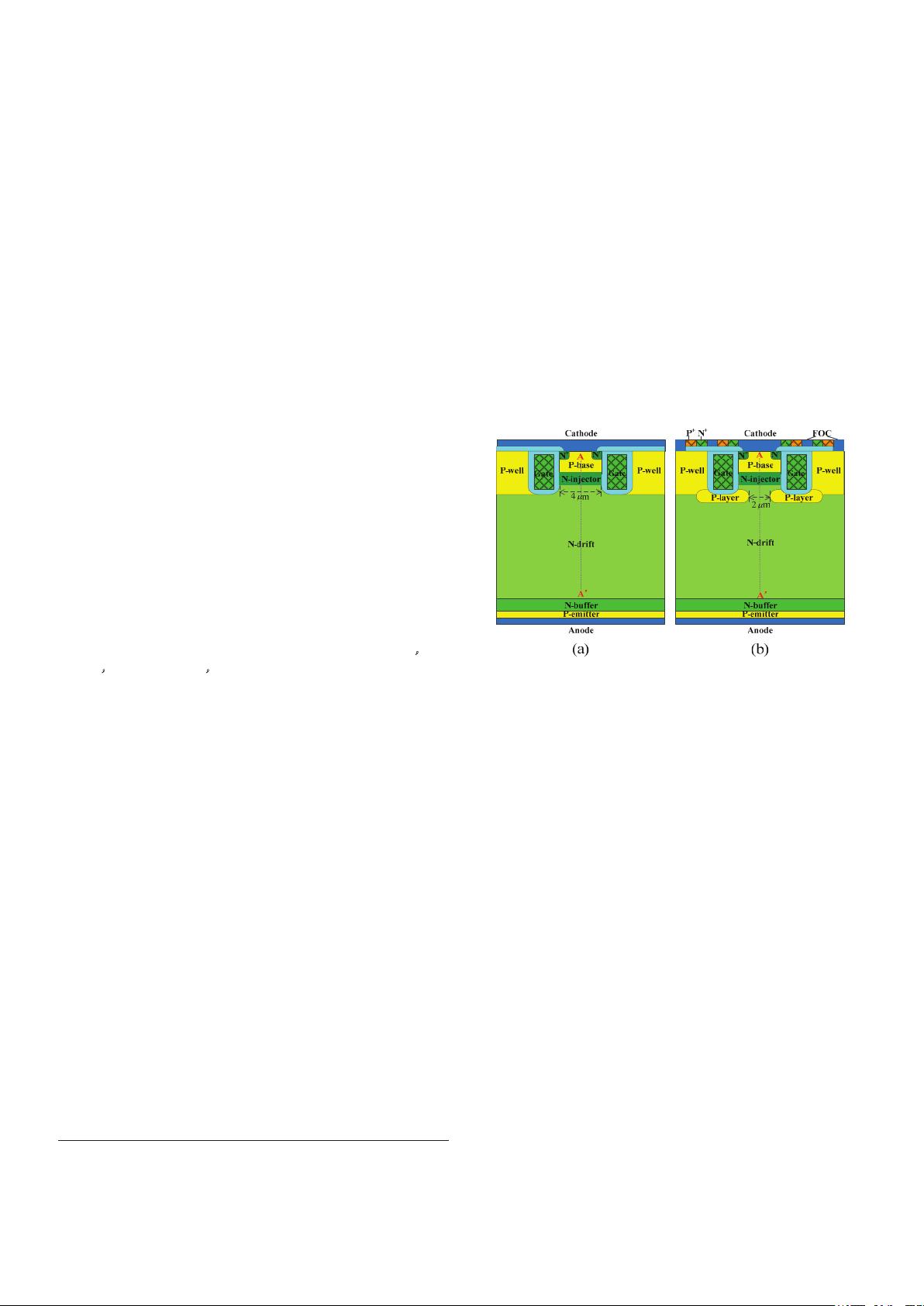
Fig. 1. Schematic section views of: (a) conventional CSTBT and (b) the
proposed CSTBT.
II. D
EVICE
S
TRUCTURE
A
ND
A
NALYSIS
Fig. 1 shows the cross section view of the conventional
CSTBT and the proposed one. They have the same structure
except that the P-layer and the integrated series diodes which
are employed in the proposed CSTBT. However, the P-well
region is completely floating in the conventional CSTBT,
while the P-well region of the proposed CSTBT connecting
with the P-layer region is connected to the cathode electrode
through two integrated series diodes. The floating ohmic
contact electrode is used to connect the diodes to the P-well
region and also to connect the diode to diode. The P-layer
region of the proposed CSTBT locates under trench gate and
the integrated series diodes are implemented by the poly-
silicon layer on field oxide [12].
In the blocking-state, both P-base/N-injector junction and
P-layer/N-drift junction are reverse biased. Due to the low
doping concentration and small gap width between the two
adjacent P-layer regions, the N-drift region which is under the
N-injector region can be easily fully depleted before P-base/N-
injector junction breakdown happens, which makes the
potential of the N-injector region barely increases with the
anode voltage, thus the P-base/N-injector junction does not
sustain the reverse voltage any more. And then most of the
Project supported by the State Key Program of National Natural Science
of China(Grant No. 51237001) and the National Science Foundation of China
for Young Scholars (Grant No. 61504021).


