
16
LMK03328
ZHCSE36D –AUGUST 2015–REVISED APRIL 2018
www.ti.com.cn
Copyright © 2015–2018, Texas Instruments Incorporated
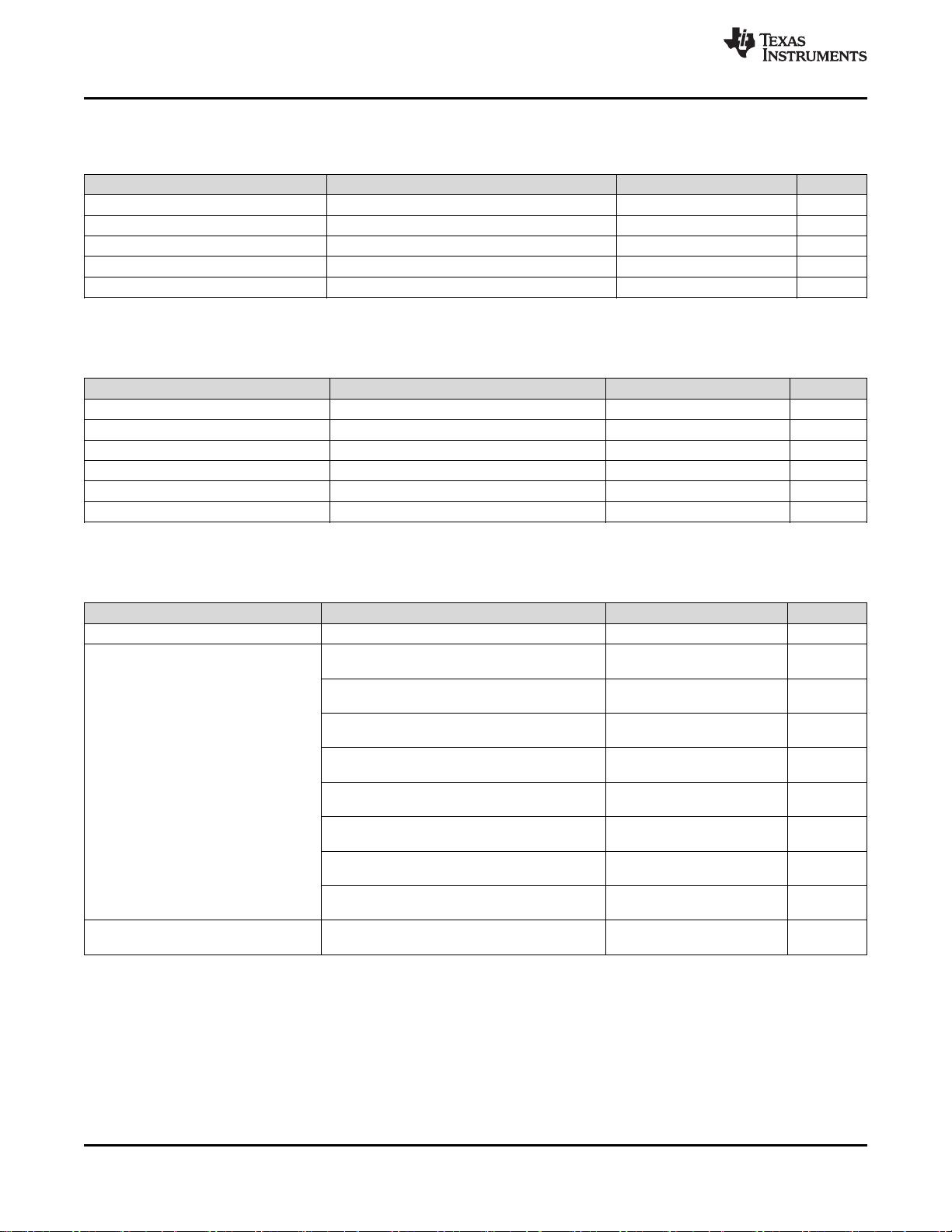
8.20 2-Level Logic Input Characteristics (HW_SW_CTRL, PDN, GPIO[5:0])
VDD_IN / VDD_PLL1 / VDD_PLL2 / VDD_DIG = 3.3 V ± 5%, VDDO_x = 1.8 V ± 5%, 2.5 V ± 5%, 3.3 V ± 5%, T
A
= –40°C to
85°C
PARAMETER TEST CONDITIONS MIN TYP MAX UNIT
V
IH
Input High Voltage 1.2 V
V
IL
Input Low Voltage 0.6 V
I
IH
Input High Current V
IH
= VDD_DIG –40 40 µA
I
IL
Input Low Current V
IL
= GND –40 40 µA
C
IN
Input Capacitance 2 pF
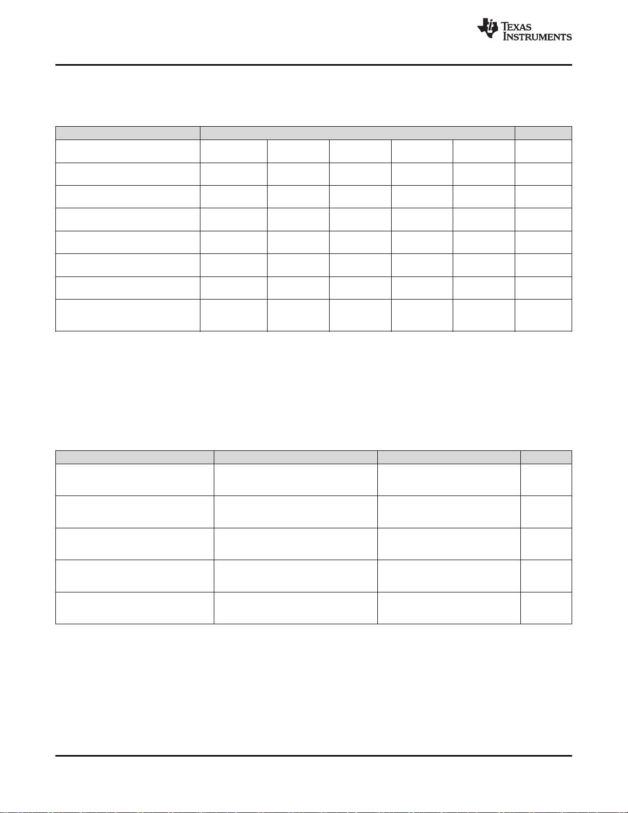
8.21 3-Level Logic Input Characteristics (REFSEL, GPIO[3:1])
VDD_IN / VDD_PLL1 / VDD_PLL2 / VDD_DIG = 3.3 V ± 5%, VDDO_x = 1.8 V ± 5%, 2.5 V ± 5%, 3.3 V ± 5%, T
A
= –40°C to
85°C
PARAMETER TEST CONDITIONS MIN TYP MAX UNIT
V
IH
Input High Voltage 1.4 V
V
IM
Input Mid Voltage 0.9 V
V
IL
Input Low Voltage 0.4 V
I
IH
Input High Current V
IH
= VDD_DIG –40 40 µA
I
IL
Input Low Current V
IL
= GND –40 40 µA
C
IN
Input Capacitance 2 pF
8.22 Analog Input Characteristics (GPIO[5])
VDD_IN / VDD_PLL1 / VDD_PLL2 / VDD_DIG = 3.3 V ± 5%, VDDO_x = 1.8 V ± 5%, 2.5 V ± 5%, 3.3 V ± 5%, T
A
= –40°C to
85°C, pulldown resistor on GPIO[5] to GND as specified below, HW_SW_CTRL = 0
PARAMETER TEST CONDITIONS MIN TYP MAX UNIT
V
ctrl
Control voltage range 0 VDD_DIG V
V
IN_XOOF
FSET_STEP
Input Voltage for XO
Frequency Offset Step
Selection on GPIO[5]
50 Ω to GND: Selects on-chip capacitive load set
by R88 and R89
50 mV
2.32 kΩ to GND: Selects on-chip capacitive load
set by R90 and R91
200 mV
5.62 kΩ to GND: Selects on-chip capacitive load
set by R92 and R93
400 mV
10.5 kΩ to GND: Selects on-chip capacitive load
set by R94 and R95
600 mV
18.7 kΩ to GND: Selects on-chip capacitive load
set by R96 and R97
800 mV
34.8 kΩ to GND: Selects on-chip capacitive load
set by R98 and R99
1000 mV
84.5 kΩ to GND: Selects on-chip capacitive load
set by R100 and R101
1200 mV
Left floating: Selects on-chip capacitive load set
by R102 and R103
1400 mV
t
DELAY
Delay between voltage
changes on GPIO[5] pin
100 ms


剩余153页未读,继续阅读

不觉明了
- 粉丝: 3281
- 资源: 5614
 我的内容管理
收起
我的内容管理
收起
- 我的资源
快来上传第一个资源
 我的收益 登录查看自己的收益
 我的积分
登录查看自己的积分
我的积分
登录查看自己的积分
 我的C币
登录后查看C币余额
我的C币
登录后查看C币余额
 我的收藏
我的收藏  我的下载
我的下载  下载帮助
下载帮助

会员权益专享


最新资源
- Simulink在电机控制仿真中的应用
- 电子警察:功能、结构与抓拍原理详解
- TESSY 4.1 英文用户手册:Razorcat Development GmbH
- 5V12V直流稳压电源设计及其实现
- 江西建工四建来宾市消防支队高支模施工方案
- 三维建模教程:创建足球模型
- 宏福苑南二区公寓楼施工组织设计
- 福建外运集团信息化建设技术方案:网络与业务平台设计
- 打造理想工作环境:详尽的6S推行指南
- 阿里巴巴数据中台建设与实践
- 欧姆龙CP1H PLC操作手册:SYSMACCP系列详解
- 中国移动统一DPI设备技术规范:LTE数据合成服务器关键功能详解
- 高校竞赛信息管理系统:软件设计与体系详解
- 面向对象设计:准则、启发规则与系统分解
- 程序设计基础与算法解析
- 算法与程序设计基础概览
资源上传下载、课程学习等过程中有任何疑问或建议,欢迎提出宝贵意见哦~我们会及时处理!
点击此处反馈


