
16
MSP430F5529
,
MSP430F5528
,
MSP430F5527
,
MSP430F5526
MSP430F5525
,
MSP430F5524
,
MSP430F5522
,
MSP430F5521
MSP430F5519, MSP430F5517, MSP430F5515, MSP430F5514, MSP430F5513
SLAS590N –MARCH 2009–REVISED SEPTEMBER 2018
www.ti.com
Submit Documentation Feedback
Product Folder Links: MSP430F5529 MSP430F5528 MSP430F5527 MSP430F5526 MSP430F5525 MSP430F5524
MSP430F5522 MSP430F5521 MSP430F5519 MSP430F5517 MSP430F5515 MSP430F5514 MSP430F5513
Terminal Configuration and Functions Copyright © 2009–2018, Texas Instruments Incorporated
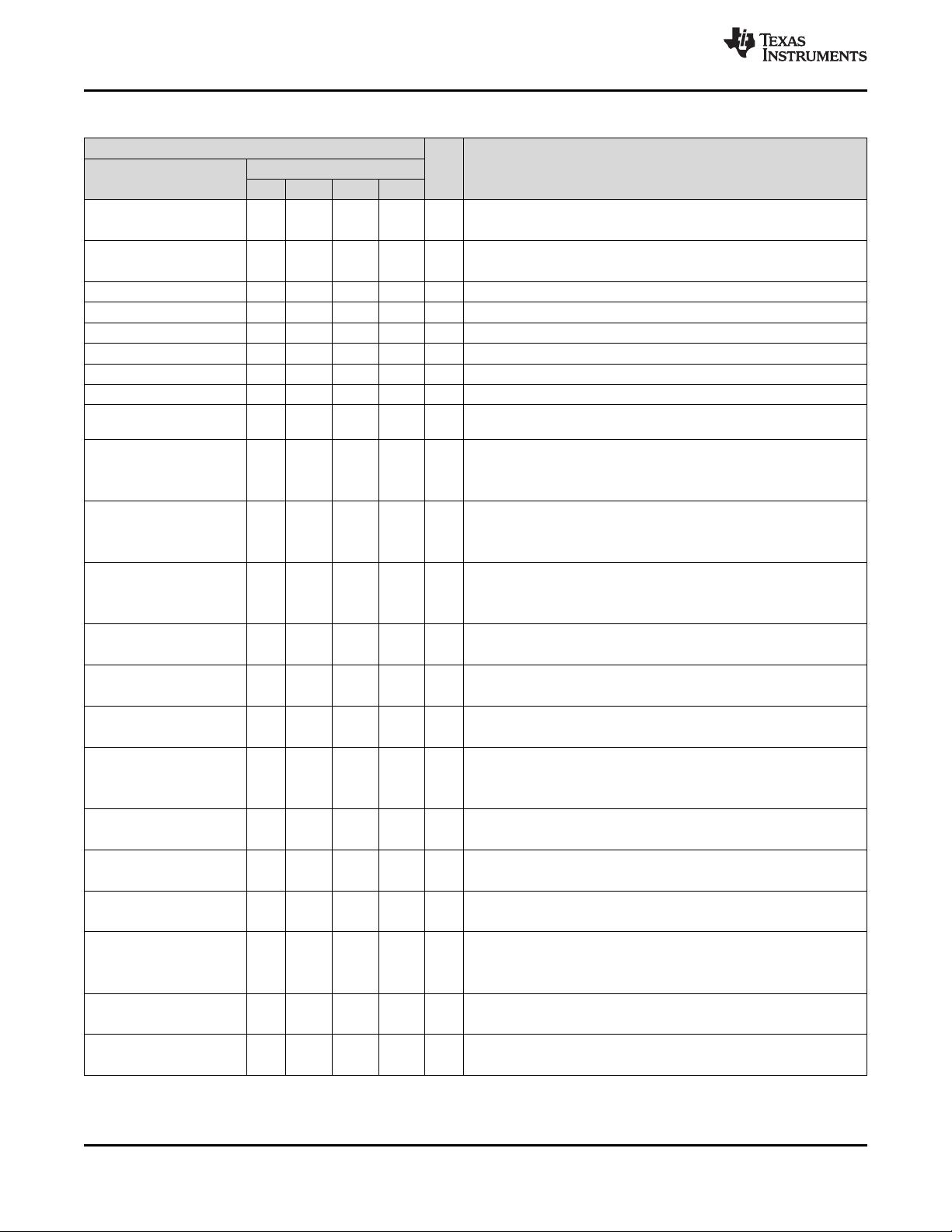
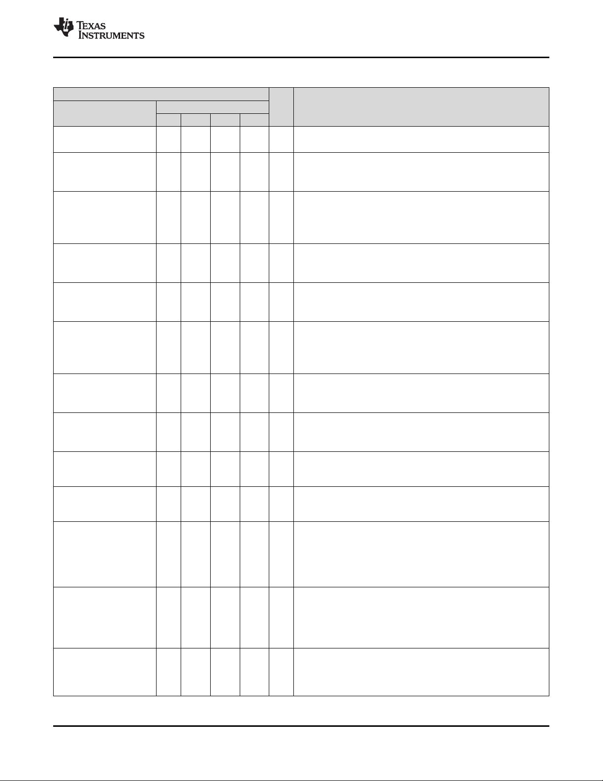
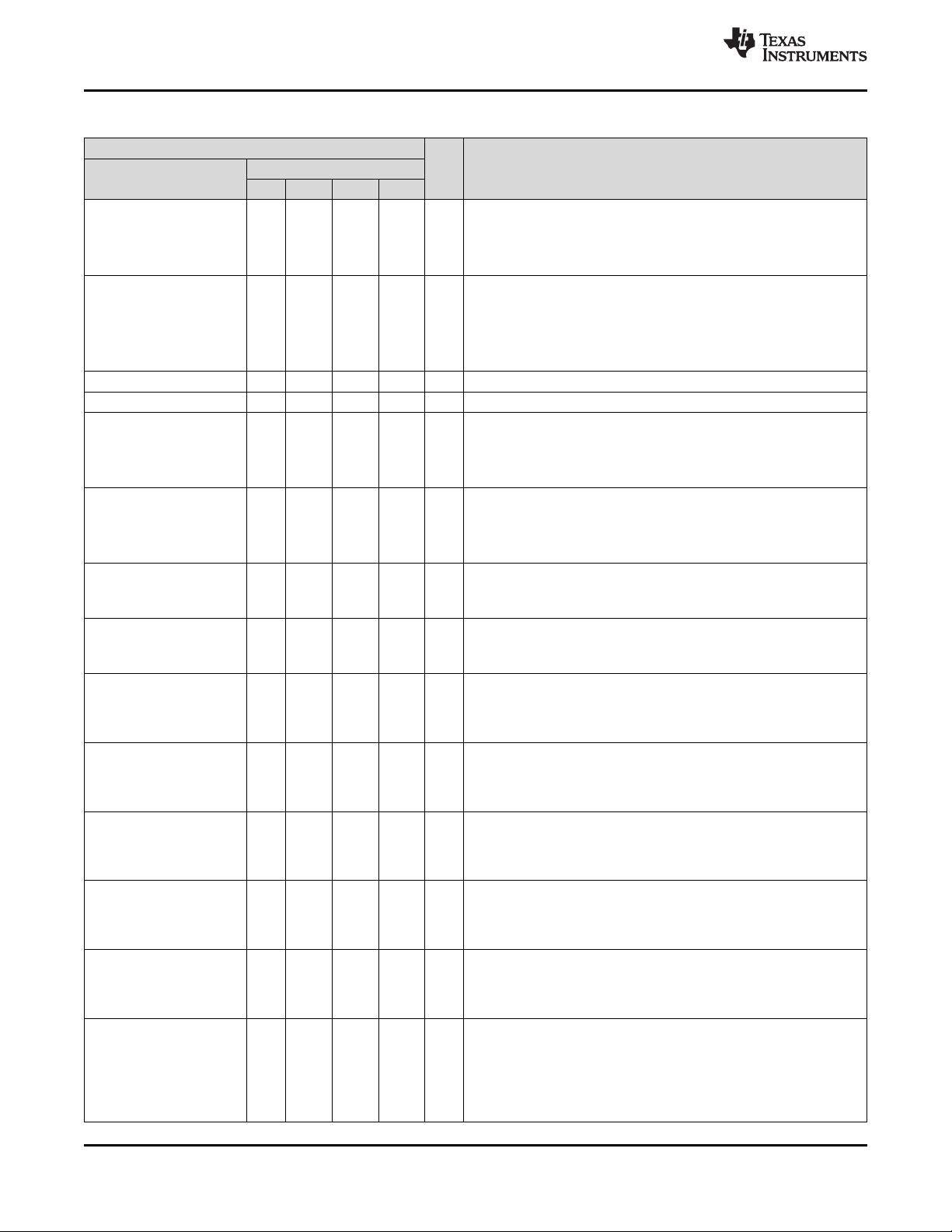
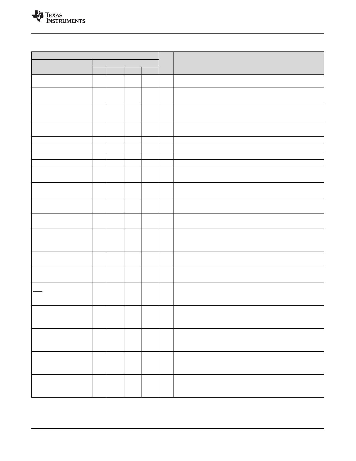
Table 4-1. Terminal Functions (continued)
TERMINAL
I/O
(1)
DESCRIPTION
NAME
NO.
PN RGC YFF ZQE
(2) VCORE is for internal use only. No external current loading is possible. Connect VCORE to the recommended capacitor value, C
VCORE
(see Section 5.3).
P5.4/XIN 12 12 A5 F1 I/O
General-purpose digital I/O
Input terminal for crystal oscillator XT1
P5.5/XOUT 13 13 A6 G1 I/O
General-purpose digital I/O
Output terminal of crystal oscillator XT1
AVSS1 14 14 A4 G2 Analog ground supply
P8.0 15 N/A N/A N/A I/O General-purpose digital I/O
P8.1 16 N/A N/A N/A I/O General-purpose digital I/O
P8.2 17 N/A N/A N/A I/O General-purpose digital I/O
DVCC1 18 15 A7 H1 Digital power supply
DVSS1 19 16 A8 J1 Digital ground supply
VCORE
(2)
20 17 B8 J2
Regulated core power supply output (internal use only, no external
current loading)
P1.0/TA0CLK/ACLK 21 18 B7 H2 I/O
General-purpose digital I/O with port interrupt
TA0 clock signal TA0CLK input
ACLK output (divided by 1, 2, 4, 8, 16, or 32)
P1.1/TA0.0 22 19 B6 H3 I/O
General-purpose digital I/O with port interrupt
TA0 CCR0 capture: CCI0A input, compare: Out0 output
BSL transmit output
P1.2/TA0.1 23 20 C6 J3 I/O
General-purpose digital I/O with port interrupt
TA0 CCR1 capture: CCI1A input, compare: Out1 output
BSL receive input
P1.3/TA0.2 24 21 C8 G4 I/O
General-purpose digital I/O with port interrupt
TA0 CCR2 capture: CCI2A input, compare: Out2 output
P1.4/TA0.3 25 22 C7 H4 I/O
General-purpose digital I/O with port interrupt
TA0 CCR3 capture: CCI3A input compare: Out3 output
P1.5/TA0.4 26 23 D6 J4 I/O
General-purpose digital I/O with port interrupt
TA0 CCR4 capture: CCI4A input, compare: Out4 output
P1.6/TA1CLK/CBOUT 27 24 D7 G5 I/O
General-purpose digital I/O with port interrupt
TA1 clock signal TA1CLK input
Comparator_B output
P1.7/TA1.0 28 25 D8 H5 I/O
General-purpose digital I/O with port interrupt
TA1 CCR0 capture: CCI0A input, compare: Out0 output
P2.0/TA1.1 29 26 E5 J5 I/O
General-purpose digital I/O with port interrupt
TA1 CCR1 capture: CCI1A input, compare: Out1 output
P2.1/TA1.2 30 27 E8 G6 I/O
General-purpose digital I/O with port interrupt
TA1 CCR2 capture: CCI2A input, compare: Out2 output
P2.2/TA2CLK/SMCLK 31 28 E7 J6 I/O
General-purpose digital I/O with port interrupt
TA2 clock signal TA2CLK input
SMCLK output
P2.3/TA2.0 32 29 E6 H6 I/O
General-purpose digital I/O with port interrupt
TA2 CCR0 capture: CCI0A input, compare: Out0 output
P2.4/TA2.1 33 30 F8 J7 I/O
General-purpose digital I/O with port interrupt
TA2 CCR1 capture: CCI1A input, compare: Out1 output
剩余132页未读,继续阅读

默然_无畏
- 粉丝: 49
- 资源: 22
 我的内容管理
展开
我的内容管理
展开


最新资源
- 最优条件下三次B样条小波边缘检测算子研究
- 深入解析:wav文件格式结构
- JIRA系统配置指南:代理与SSL设置
- 入门必备:电阻电容识别全解析
- U盘制作启动盘:详细教程解决无光驱装系统难题
- Eclipse快捷键大全:提升开发效率的必备秘籍
- C++ Primer Plus中文版:深入学习C++编程必备
- Eclipse常用快捷键汇总与操作指南
- JavaScript作用域解析与面向对象基础
- 软通动力Java笔试题解析
- 自定义标签配置与使用指南
- Android Intent深度解析:组件通信与广播机制
- 增强MyEclipse代码提示功能设置教程
- x86下VMware环境中Openwrt编译与LuCI集成指南
- S3C2440A嵌入式终端电源管理系统设计探讨
- Intel DTCP-IP技术在数字家庭中的内容保护
资源上传下载、课程学习等过程中有任何疑问或建议,欢迎提出宝贵意见哦~我们会及时处理!
点击此处反馈


