C
7/01
TNY253/254/255
4
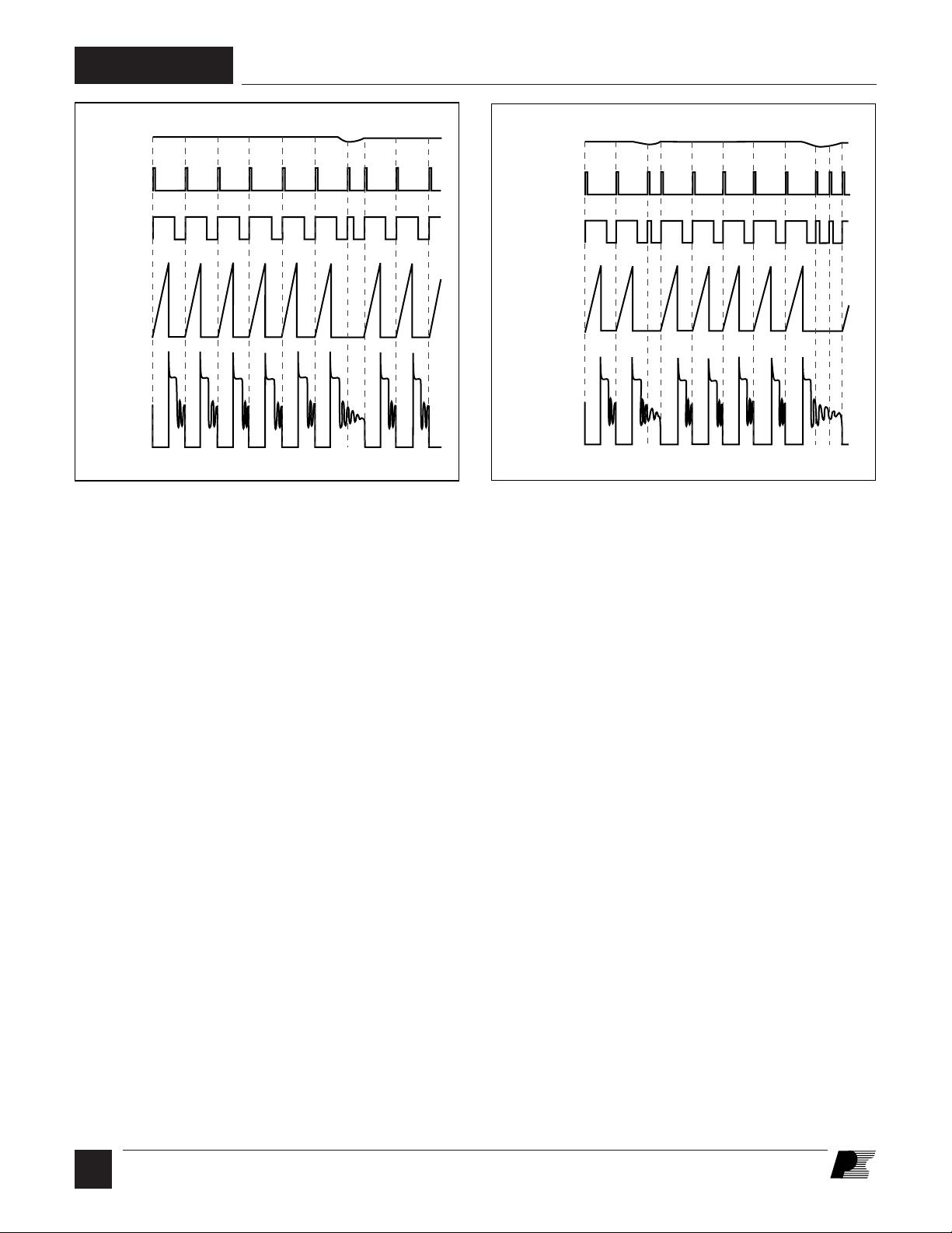
Figure 4. TinySwitch Operation at Heavy Load. Figure 5. TinySwitch Operation at Medium Load.
V
DRAIN
V
EN
CLOCK
DC
DRAIN
I
MAX
PI-2255-061298
V
DRAIN
V
EN
CLOCK
DC
DRAIN
I
MAX
PI-2259-061298
percentage of cycles will conduct to support the power
consumption of the power supply.
The response time of TinySwitch ON/OFF control scheme is
very fast compared to normal PWM control. This provides high
line ripple rejection and excellent transient response.
Power Up/Down
TinySwitch requires only a 0.1 µF capacitor on the BYPASS
pin. Because of the small size of this capacitor, the power-up
delay is kept to an absolute minimum, typically 0.3 ms (Figure7).
Due to the fast nature of the ON/OFF feedback, there is no
overshoot at the power supply output. During power-down, the
power MOSFET will switch until the rectified line voltage
drops to approximately 12 V. The power MOSFET will then
remain off without any glitches (Figure 8).
Bias Winding Eliminated
TinySwitch does not require a bias winding to provide power to
the chip. Instead it draws the power directly from the DRAIN
pin (see Functional Description above). This has two main
benefits. First for a nominal application, this eliminates the cost
of an extra bias winding and associated components. Secondly,
for charger applications, the current-voltage characteristic often
allows the output voltage to fall to low values while still
delivering power. This type of application normally requires a
forward-bias winding which has many more associated
components, none of which are necessary with TinySwitch.
Current Limit Operation
Each switching cycle is terminated when the DRAIN current
reaches the current limit of the TinySwitch. For a given primary
inductance and input voltage, the duty cycle is constant.
However, duty cycle does change inversely with the input
voltage providing “voltage feed-forward” advantages: good
line ripple rejection and relatively constant power delivery
independent of the input voltage.
44 kHz Switching Frequency (TNY253/254)
Switching frequency (with no cycle skipping) is set at 44kHz.
This provides several advantages. At higher switching
frequencies, the capacitive switching losses are a significant
proportion of the power losses in a power supply. At higher
frequencies, the preferred snubbing schemes are RCD or diode-
Zener clamps. However, due to the lower switching frequency
of TinySwitch , it is possible to use a simple RC snubber (and
even just a capacitor alone in 115VAC applications at powers
levels below 4W).
Secondly, a low switching frequency also reduces EMI filtering
requirements. At 44kHz, the first, second and third harmonics
are all below 150kHz where the EMI limits are not very
restrictive. For power levels below 4W it is possible to meet
worldwide EMI requirements with only resistive and capacitive
filter elements (no inductors or chokes). This significantly
reduces EMI filter costs.
Finally, if the application requires stringent noise emissions
(such as video applications), then the TNY253/254 will allow
more effective use of diode snubbing (and other secondary
snubbing techniques). The lower switching frequency allows
RC snubbers to be used to reduce noise, without significantly
impacting the efficiency of the supply.


