An Analytic Potential Based Model for Gate-All-Around Nanowire Tunnel-FETs
Ying Liu
*
, Jin He
*
, Mansun Chan
**
, Caixia Du
***
, Yun Ye
*
, Wei Zhao
*
, Wen Wu
*
, and Wenping Wang
*
*
Peking University Shenzhen SOC Key Laboratory, PKU-HKUST Shenzhen-Hong Kong Institution,
Shenzhen, China
**
Department of Electronic and Computer Engineering, Hong Kong University of Science and Technology,
Kowloon, Hong Kong
***
Shenzhen Huayue Teracale Chip Electronic Limited Co., Shenzhen, China
ABSTRACT
In this paper, an analytic potential based current model of
the gate-all-around (GAA) silicon nanowire tunnel-FETs
(NW-TFETs) is proposed based on the surface potential
solutions at the channel direction and considering band to
band tunneling (BTBT) efficiency. The 3-D Poisson’s
equation is solved to obtain the surface potential distribution
in the partition regions along the channel direction for
NW-TFET device and then a tunneling current model using
Kane’s expression is developed. The validity of the developed
model is proved by the good agreement between the model
predictions and TCAD simulation results.
Keywords: Gate-All-Around (GAA); nanowire tunnel-FETs
(NW-TFETs); band to band tunneling (BTBT); analytic
model.
1 INTRODUCTION
Tunnel-FETs (TFET) has been got great attention in the
semiconductor academic and industry fields in recent years
for the superior performance in sub-threshold region.
Compared with the conventional MOSFETs, TFET is
competitive and chosen due to its high ON-OFF current ratio,
below 60 mV/dec sub-threshold swing (SS) and low leakage
power consumption [1-4]. However, TFETs have a small
amount of band to band tunneling (BTBT) efficiency in the
large band gap of silicon body leading to a low ON-current.
To obtain the high ON-current and small SS, the GAA
NW-TFETs is considered as an efficient device candidate.
NW-TFET process technology and fabrication measures have
been matured recently and many research papers have been
published [4-6]. However, the compact model of NW-TFET
for circuit performance prediction and simulation has made a
few progresses. Most works only focus on NW-TFET
empirical model development [5,9]. So far, there is no a
complete analytical model of GAA NW-TFET for device
scientists and circuit designers to test and simulation such a
device based circuit performance.
In this paper, an analytical model of GAA silicon
NW-TFETs has been developed based on the
three-dimensional (3-D)
potential solution and the Kane’s
expression. For observing the validity of the model and the
different parameters impact on the device performance, we
have also compared the analytical model prediction with
the TCAD SenTaurus simulation results of the device to
verify the model validity.
2 STRUCTURE AND MODEL
2.1 Structure of GAA NW-TFET
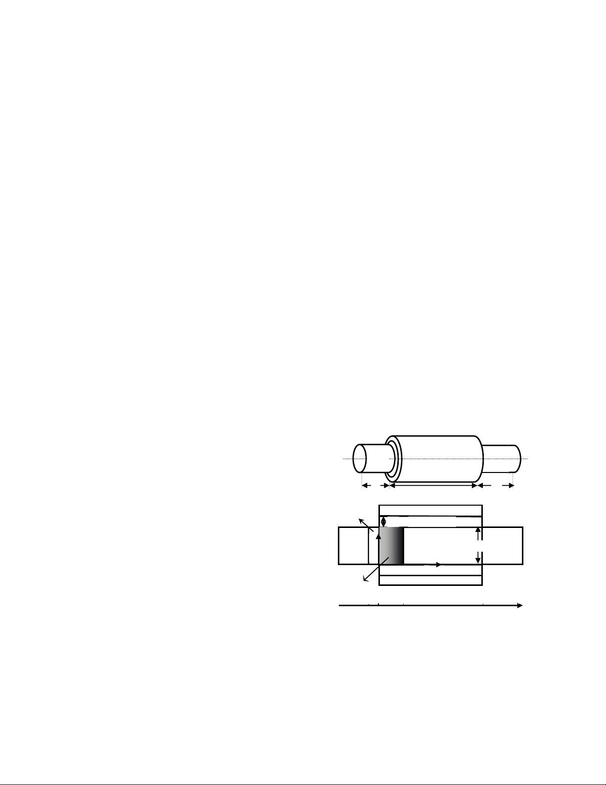
The Figure1 shows the structure of GAA TFET with
silicon nanowire body. Figure1 (a) indicates 3-D structure of
the n-channel GAA NW-TFET. Figure1 (b) represents the
cross-section of the device with n-channel. In this paper,
n-TFET is considered so the doping profile along the axis
direction with the
p
doping in source,
n
doping in channel
and drain. Band-to-band tunneling (BTBT) happens in the
P/N junction at the source/channel region. Based on the
drift-diffusion (DD) theory, the electrons are moved toward
the drain thus the device can be divided into three regions: the
depletion region , the tunneling region and the surplus
channel region .
Figure 1: (a) 3-D structure of the n-channel GAA Silicon
NW-TFET (b) Cross-section of the device and its division
into a depletion region , a tunneling region
conventional GAA MOSFET region
Energy bands with electron and hole quasi-Fermi energies
along the axis direction from the device simulator TCAD
SenTaurus are
demonstrated in Figure2. As shown, inversion


